NC393 progress update: all hardware is operational
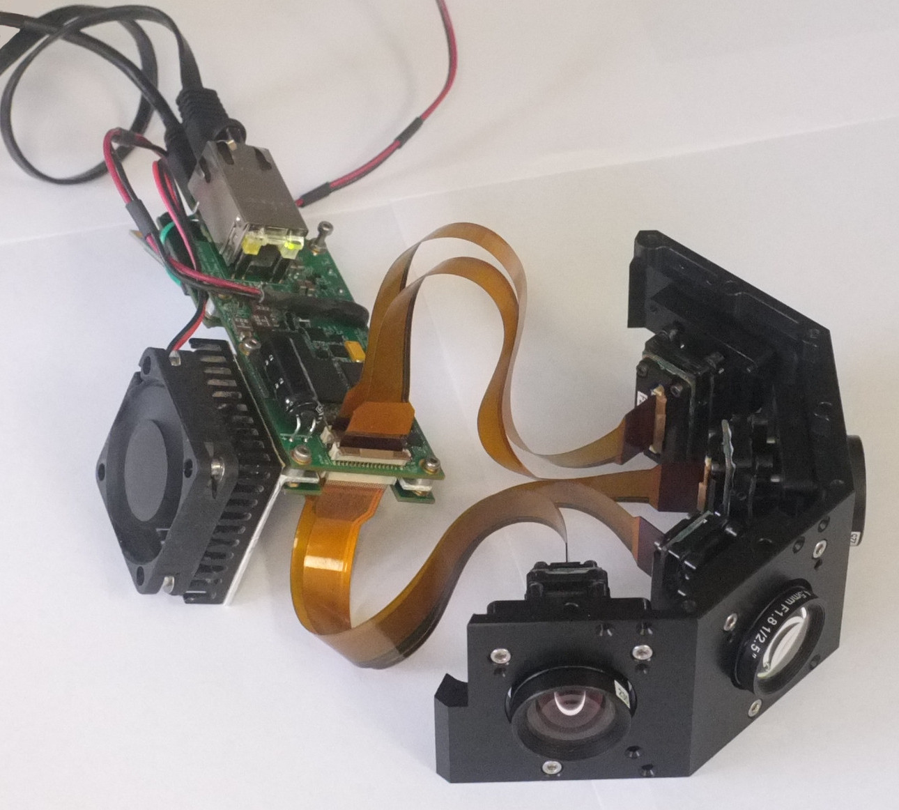
10393 with 4 image sensors
Contents
Implementation of the 16-channel DDR3 memory controller
Getting to the next part – testing of the FPGA-controlled DDR3 memory took us longer: the overall concept and the physical layer were implemented in June 2014, timing calibration software and application modules for image image recording and retrieval were implemented in the spring of 2015.
Initial image acquisition and compression
When the memory was proved operational what remained untested on the board were the sensor connections and the high speed serial links for SATA. I decided not to make any temporary modules just to check the sensor physical connections but to port the complete functionality of the image acquisition, processing and compression of the existing NC353 camera (just at a higher clock rate and multiple channels instead of a single one) and then test the physical operation together with all the code.
Sensor acquisition channels: From the sensor interface to the video memory buffer
The image acquisition code was ported (or re-written) in June, 2015. This code includes:
- Sensor physical interface – currently for the existing 10338 12-bit parallel sensor front ends, with provisions for the up to 8-lanes + clock high speed serial sensors to be added. It is also planned to bond together multiple sensor channels to interface single large/high speed sensor
- Data and clock synchronization, flexible phase adjustment to recover image data and frame format for different camera configurations, including sensor multiplexers such as the 10359 board
- Correction of the lens vignetting and fine-step scaling of the pixel values, individual for each of the multiplexed sensors and color channel
- Programmable gamma-conversion of the image data
- Writing image data to the DDR3 image buffer memory using one or several frame buffers per channel, both 8bpp and 16bpp (raw image data, bypassing gamma-conversion) formats are supported
- Calculation of the histograms, individual for each color component and multiplexed sensor
- Histograms multiplexer and AXI interface to automatically transfer histogram data to the system memory
- I²c sequencer controls image sensors over i²c interface by applying software-provided register changes when the designated frame starts, commands can be scheduled up to 14 frames in advance
- Command frame sequencer (one per each sensor channel) schedules and applies system register writes (such as to control compressors) synchronously to the sensors frames, commands can be scheduled up to 14 frames in advance
JPEG/JP4 compression functionality
Image compressors get the input data from the external video buffer memory organized as 16×16 pixel macroblocks, in the case of color JPEG images larger overlapping tiles of 18×18 (or 20×20) pixels are needed to interpolate “missing” colors from the input Bayer mosaic input. As all the data goes through the buffer there is no strict requirement to have the same number of compressor and image acquisition modules, but the initial implementation uses 1:1 ratio and there are 4 identical compressor modules instantiated in the design. The compressor output data is multiplexed between the channels and then transferred to the system memory using 1 or 2 of Xilinx Zynq AXI HP interfaces.
This portion of the code is also based on the earlier design used in the existing NC353 camera (some modules are reusing code from as early as 2002), the new part of the code was dealing with a flexible memory access, older cameras firmware used hard-wired 20×20 pixel tiles format. Current code contains four identical compressor channels providing JPEG/JP4 compression of the data stored in the dedicated DDR3 video buffer memory and then transferring result to the system memory circular buffers over one or two of the Xilinx Zynq four AXI HP channels. Other camera applications that use sensor data for realtime processing rather than transferring all the image data to the host may reduce number of the compressors. It is also possible to use multiple compressors to work on a single high resolution/high frame rate sensor data stream.
Single compressor channel contains:
- Macroblock buffer interface requests 32×18 or 32×16 pixel tiles from the memory and provides 18×18 overlapping macroblocks for JPEG or 16×16 non-overlapping macroblocks for JP4 using 4KB memory buffer. This buffer eliminates the need to re-read horizontally overlapping pixels when processing consecutive macroblocks
- Pixel buffer interface retrieves data from the memory buffer providing sequential pixel stream of 18×18 (16×16) each macroblock
- Color conversion module selects one of the sub-modules : csconvert18a, csconvert_mono, csconvert_jp4 or csconvertjp4_diff to convert possibly overlapping Bayer mosaic tiles to a sequence of 8×8 blocks for 2-d DCT transform
- Average value extractor calculates average value in each 8×8 block, subtracts it before DCT and restores after – that reduces data width in DCT processing module
- xdct393 performs 2-d DCT for each 8×8 pixel block
- Quantizer re-orders each block DCT components from the scan-line to zigzag sequence and quantizes them using software-calculated and loaded tables. This is the only lossy stage of the JPEG algorithm, when the compression quality is set to 100% all the coefficients are set to 1 and the conversion is lossless
- Focus sharpness module accumulates amount of high-frequency components to estimate image sharpness over specified window to facilitate (auto) focusing. It also allows to replace on-the-fly average block value of the image with amount of the high frequency components in the same blog, providing visual indication of the focus sharpness
- RLL encoder converts the continuous 64 samples/per block data stream in to RLL-encoded data bursts
- Huffman encoder uses software-generated tables to provide additional lossless compression of the RLL-encoded data. This module (together with the next one) runs and double pixel clock rate and has an input FIFO between the clock domains
- Bit stuffer consolidates variable length codes coming out from the Huffman encoder into fixed-width words, escaping each 0xff byte (these bytes have special meaning in JPEG stream) by inserting 0x00 right after it. It additionally provides image timestamp and length in bytes after the end of the compressed data before padding the data to multiple of 32-byte chunks, this metadata has fixed offset before the 32-byte aligned data end
- Compressor output FIFO converts 16-bit wide data from the bit stuffer module received at a double compressor clock rate (currently 200MHz) and provides 64-bit wide output at the maximal clock rate (150MHz) for AXI HP port of Xilinx Zynq, it also provides buffering when several compressor channels share the same AXI HP channel
Another module – 4:1 compressor multiplexer is shared between multiple compressor channels. It is possible (defined by Verilog parameters) to use either single multiplexer with one AXI HP port (SAXIHP1) and 4 compressor inputs (4:1), or two of these modules interfacing two AXI HP channels (SAXIHP1 and SAXIHP2), reducing number of concurrent inputs of each multiplexer to just 2 (2 × 2:1). Multiplexers use fair arbitration policy and consolidate AXI bursts to full 16×64bits when possible. Status registers provide image data pointers for last write and last frame start, each as sent to AXI and after confirmation using AXI write response channel.
Porting remaining FPGA functionality to the new camera
Additional modules where ported to complete the existing NC353 functionality:
- Camera real time clock that provides current time with 1 microsecond resolution to various modules. It has accumulator-based correction circuitry to compensate for crystal oscillator frequency variations
- Inter-camera synchronization module generates and/or receives synchronization signals between multiple camera modules or other devices. When used between the cameras, each synchronization pulse has a timestamp information attached in a serialized form, so multiple synchronized cameras have all the simultaneous images metadata contain the same time code generated by the “master” camera
- Event logger records data from multiple sources, such as GPS, IMU, image acquisition events and external signal channel (like a vehicle wheel rotation sensor)
Simulating the full codebase
All that code was written (either new or modified from the existing NC353 FPGA project by the end of July, 2015 and then the most fun began. First I used the proven NC353 code to simulate (using Icarus Verilog + GtkWave) with the same input data as the one provided to the new x393 code, following the signal chains and making sure that each checkpoint data matched. That was especially useful when debugging JPEG compressor, as the intermediate data is difficult to follow. When I was developing the first JPEG compressor in 2002 I had to save output data from the various processing stages and compare it to the software compression output of the same image data from the similar stages. Having working implementation helped a lot and in 3 weeks I was able to match the output from all the processing stages described above except the event logger that I did not verify yet.
Testing the hardware
Then it was the time for translating the Verilog test fixture code to the Python programs running on the target hardware extending the code developed earlier for the memory controller. The code is able to parse Verilog parameter definition files – that simplified synchronization of the Verilog and Python code. It would be nice to use something like Cocotb in the future and completely get rid of the Verilog to Python manual translation.
As I am designing code for the reconfigurable FPGA (not for ASIC) my usual strategy is not to get high simulation coverage, but to simulate to a “barely working” stage, then use the actual hardware (that runs tens of millions times faster than the simulator), detect the problems and then try to achieve the same condition with the simulation. But when I just started to run the hardware I realized that there is too little I can get about the current state of the hardware. Remembering about the mess of the temporary debug code I had in the previous projects and the inability of the synthesis tool to directly access the qualified names of the signals inside sub-modules, I implemented rather simple debug infrastructure that uses a single register ring (like a simplified JTAG) through all the modules to debug and a matching Python code that allows access to individual bit fields of the ring. Design includes a single debug_master and debug_slave modules in each of the design module instances that needs debugging (and the modules above – up to the top one). By the time the camera was able to generate correct images the total debug ring consisted of almost a hundred of the 32-bit registers, when I later disabled this debug functionality by commenting out a single `define DEBUB_RING macro it recovered almost 5% of the device slices. The program output looks like:
x393 +0.001s--> print_debug 0x38 0x3e

038.00:                     compressors393_i.jp_channel0_i.debug_fifo_in [32] = 0x6e280 (451200)

039.00:                    compressors393_i.jp_channel0_i.debug_fifo_out [28] = 0x1b8a0 (112800)

039.1c:                  compressors393_i.jp_channel0_i.dbg_block_mem_ra [ 3] = 0x3 (3)

039.1f:                compressors393_i.jp_channel0_i.dbg_comp_lastinmbo [ 1] = 0x1 (1)

03a.00:                   compressors393_i.jp_channel0_i.pages_requested [16] = 0x26c2 (9922)

03a.10:                         compressors393_i.jp_channel0_i.pages_got [16] = 0x26c2 (9922)

03b.00:                    compressors393_i.jp_channel0_i.pre_start_cntr [16] = 0x4c92 (19602)

03b.10:                      compressors393_i.jp_channel0_i.pre_end_cntr [16] = 0x4c92 (19602)

03c.00:                     compressors393_i.jp_channel0_i.page_requests [16] = 0x4c92 (19602)

03c.10:                      compressors393_i.jp_channel0_i.pages_needed [16] = 0x26c2 (9922)

03d.00:                      compressors393_i.jp_channel0_i.dbg_stb_cntr [16] = 0xcb6c (52076)

03d.10:                      compressors393_i.jp_channel0_i.dbg_zds_cntr [16] = 0xcb6c (52076)

03e.00:                  compressors393_i.jp_channel0_i.dbg_block_mem_wa [ 3] = 0x4 (4)

03e.03:             compressors393_i.jp_channel0_i.dbg_block_mem_wa_save [ 3] = 0x0 (0)
Acquiring the first images
All the problems I encountered while trying to make hardware work turned out to be reproducible (but no always easy) with the simulation and the next 3 weeks I was eliminating then one by one. When I’ve got to the 51-st version of the FPGA bitstream file (there were several more when I forgot to increment version number) camera started to produce consistently valid JPEG files.
First 4-sensor image acquired with NC393 camera
At that point I replaced a single sensor front end with no lens attached (just half of the input sensor window was covered with a tape to produce a blurry shadow in the images) with four complete SFE with lenses simultaneously using a piece of Eyesis4π hardware to point the individual sensors at the 45° angles (in portrait mode) covering 180°×60° FOV combined – it resulted in the images shown above. Sensor color gains are not calibrated (so there is visible color mismatch) and the images are not stitched together (just placed side-by-side) but i consider it to be a significant milestone in the NC393 camera development.
SATA controller status
Almost at the same time Alexey who is working on SATA controller for the camera achieved an important milestone too. His code running in Xilinx Zynq was able to negotiate and establish link with an mSATA SSD connected to the NC393 prototype. There is still a fair amount of design work ahead until we’ll be able to use this controller with the camera, but at least the hardware operation of this part of the design is verified now too.
What is next
Having all the hardware on the 10393 verified we are now able to implement minor improvements and corrections to the 3 existing boards of the NC393 camera:
- 10393 itself
- 10389 – extension board with mSATA SSD, eSATA/USB combo connector, micro-USB and synchronization I/O
- 10385 – power supply board
And then make the first batch of the new cameras that will be available for other developers and customers.
We also plane to make a new sensor board with On Semiconductor (former Aptina, former Micron) MT9F002 – 14MPix sensor with the same 1/2.3″ image format as the MT9P006 used with the current NC353 cameras. This 12-bit sensor will allow us to try multi-lane high speed serial interface keeping the same physical dimension of the sensor board and use the same lenses as we use now.
Leave a Reply