NC393 development progress – testing the hardware
10393 board, memory side
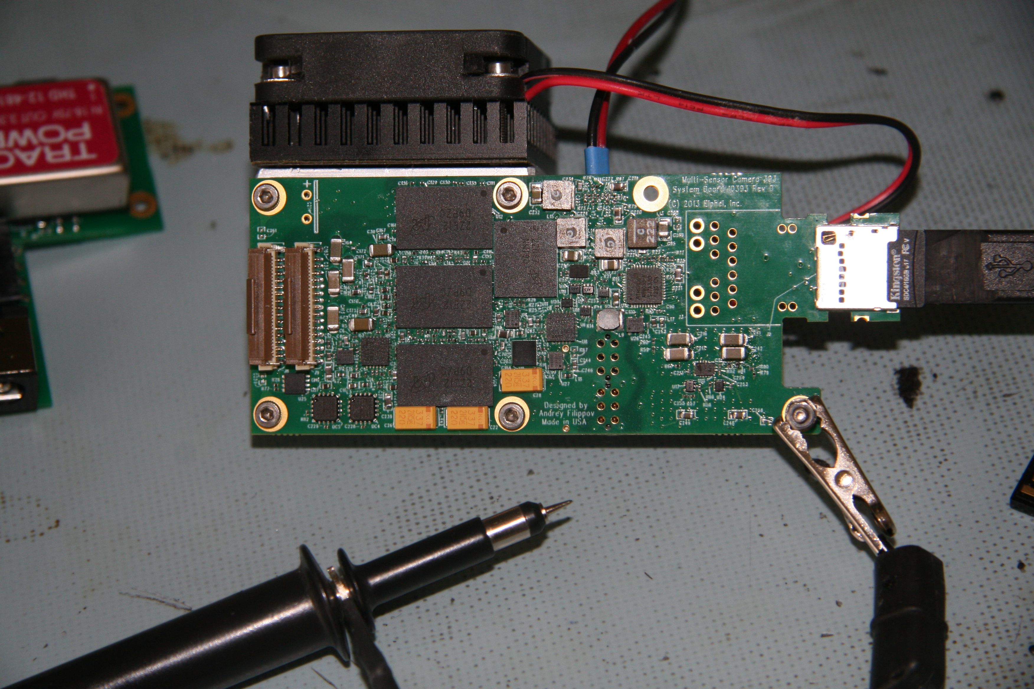
We received the first prototype of the 10393 rev.’0″ – the new camera system board with all the BGA chips mounted. It took a little longer as our PCB assembly manufacturer had to order solder paste stencils as some chips (DC-DC converter module in LGA package and QFN chips with central thermal pads) required more than just applying tacky flux and running them through the reflow oven. The photo shows the 10393 system board together with the 10385 power supply board that I assembled earlier while waiting for the main one. This time the power supply is a separate module so we’ll not need different system board versions for different power supply options as we do with Elphel current NC353.
The shown prototype version has the full functionality, including РоЕ – feature that we will not offer in the production cameras to stay out of trouble with the patent trolls. As soon as the relevant patents will be ruled invalid we will be able to build such boards, but currently the cameras will be powered through the regular barrel-type DC jack or the 4-pin Molex connector in the multi-camera systems like Eyesis. 10385 also has a low-leakage (few microamps idle consumption) switch to use the battery-powered camera in remote locations, controlled by the system clock powered by a super-capacitor (not yet installed – there is an empty space with “+” sign on visible on the photo).
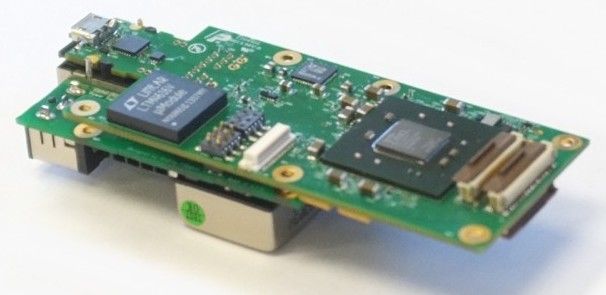
10393 with 10385 board, SoC side
I finalized the 10393 board assembly installing other components including couple hundred (bragging again) 0201 resistors and capacitors. Before starting I tested the resistance (lack of shorts) between the ground and power rails to make sure that I did not screw up pinouts during schematic/PCB design and so the board revision “0” has a chance to be successfully tested. I repeated those tests while installing components as a power-to-ground shorts are rather difficult to locate as there are so many tiny capacitors between them.
With assembly done the board was ready for the first “smoke” test – power it up while controlling the power consumption (I used a regular test bench power supply instead of the 10385 to provide the primary 3.3V power). I was turning power on for just a few seconds controlling the secondary voltages (1.0V, 1.8V and 1.5V) with the oscilloscope. After fixing a bad soldering on the intermediate “power good” pullup resistor (secondary voltages are supposed to come up in a prescribed sequence) all 3 of these voltages were up, measured OK and the board consumed 320 mA with the system reset released but no firmware to run. There are several additional DC-DC converters on board (5V for USB and 2 independently software-regulated voltages for the external boards (sensor front ends in most applications), but these converters are turned on by the software and I did not have any at the moment.
10393 board, SoC side
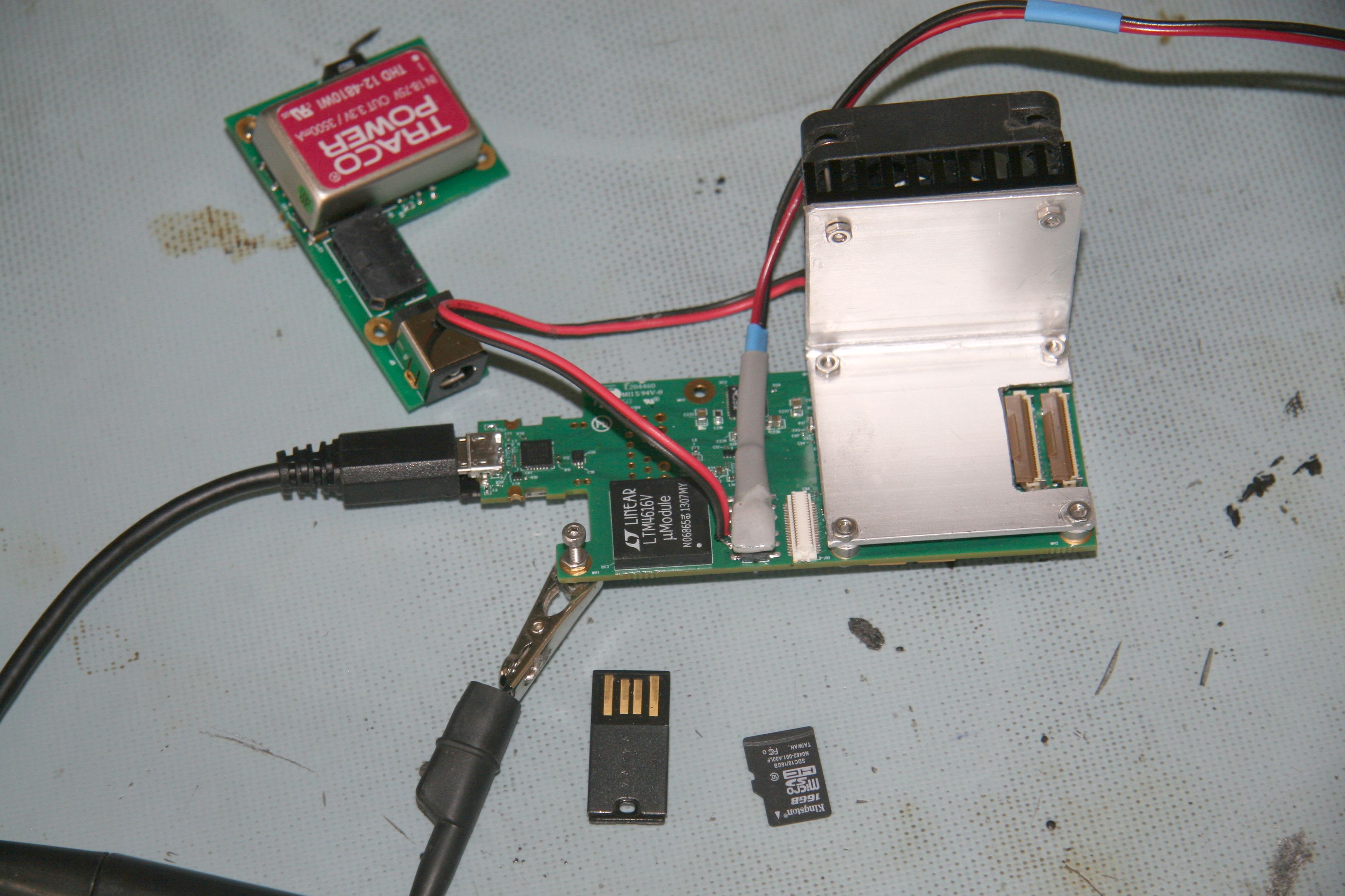
Photos show the heat sink and a fan attached to aluminum angle, not directly to the Zynq chip. In production camera there will be a custom heat sink (no fan) between the 10393 and the optional 10389 interface/storage board, it will transfer processor heat to the camera aluminum body and the on-chip thermometer will be used to monitor the temperature and prevent overheating. Rather large temporary heat sink will be used during development (not to depend on the temperature monitoring software), thin angle part will allow to test the 10389 board that will nearly touch the other surface of the aluminum plate.
The next thing to test was to make the CPU (Xilinx Zynq XC7Z030-1FBG484C) run and test the DDR3 memory. If this core of the system is operational, we can test the peripherals one by one, and failures in some of them would not prevent testing of the others. If the core would fail – we’ll have to try to find out (or just guess) the problem and redesign the board, order new ones, have new stencils, assemble and try again. Of course we’ll need to re-spin the board before the production units manufacturing, but I hoped that just the next revision will be good enough to go to the users, that changes will be small. I wrote “guessed”, because if the problems would be related to the DDR3 memory operation the means to troubleshoot them would be limited – the data and address/command lines are completely buried between the chips – memory is placed directly opposite to the Zynq SoC. There are no resistor terminations on the address/command lines, the DQ lines are swapped in each byte group and the byte groups are also swapped. I relied on Xilinx documentation that they OR-ed the data lines during write leveling, so the DQ swapping will not harm this functionality.
Skipping the requirement for the address line termination allowed the overall design to be compact and the connections themselves to be really short (actually shorter than the lines inside the SoC chip itself). I used Micron documentation when considering such solution, but it still needed to be tested on the real board. Such component placement allowed me to make average length of the address/command traces 15.5mm, individual traces had to be shortened/extended to keep combined PCB delays and internal SoC pin delays the same for each address/command and for each member in the byte group for data. Internal DDR3 chip delays do not need to be considered as they are balanced inside the package. Data connections lengths (they are just peer-to-peer, no split for the two memory chips as for address/command lines) are even shorter – they average from 8.5mm to 14.5 mm for different byte groups.
Additional challenge for the initial breathing life in this new board was that we did not have the proven code to run on it, something we had for the Avnet MicroZed board while developing the free software bootloader to replace the Xilinx proprietary one. So that was a real test for our code and I decided to never even try the proprietary one on the new system.
The 10393 board has no LED (not to count 2 Ethernet jack ones, but they are controlled by the Ethernet PHY), so I temporary borrowed one GPIO signal from the MDIO bus (Ethernet PHY control) to be able to step through the boot process not relying on the serial console to be operational. I just put the LED there without any transistor, so the 1.8V-powered diode was really dim, but that was OK. And the serial output turned out to be alive immediately so there was no real need for that debug tool and I was able to remove those extra wires. The board got to U-Boot prompt immediately, but unfortunately – not every time. So I had to spend several days (one of them because of just the faulty micro-SD card that silently replaced one sector with garbage even when read back by the computer) figuring out the instability. I still do not understand exactly what is wrong (it happens when the relocated code switches the memory mapping and copies itself back to the low addresses), but just adding delay by copying that range twice resolved the issue, it turned out to be software-related one as it was present when running other (proven) boards also, not just with the 10393.
The core of the system is now verified, automatic write leveling and the two other hardware-implemented memory training functions produce reasonable results and the delay settings seem to be rather forgiving. That confirms the PCB design and makes it possible to move forward with testing of the other peripherals and starting the FPGA part of the design.
There are other urgent projects at Elphel I have to be involved now, so not yet working on the NC393 full time, but this makes really good news for us to pass the important test. Booting the new board with just the free software, no proprietary tools at all – it is also very encouraging. Xilinx just released the new version of the tools, the human-readable (html) part of the FSBL output looks even fancier than that of Ezynq, but I believe ours is still more convenient to work with – we made it for ourselves, and so for other developers (who are like us) too.
Leave a Reply