by Oleg Dzhimiev
1. [Done] Wrote code for the FFT256 DIF.
FFT is performed in 8 conveyor organized stages. Each stage is similar to as described here. So far each stage uses 2 BRAM ports (A for 16-bit Re-part and B for 16-bit Im-part) and the 1 MULT18X18 (for the “butterfly”) – 4 BRAMs + 6 MULT18X18s (MULTs are not used in the last 2 stages). Plus other logic – 1 FFT256 uses 18% of FPGA resourses.
Each BRAM is shared by 2 stages for write and by 2 stages for read (e.g., write – stages 2,3 and read – stages 3,4) – and because the address bus is used for 4 double accesses then each channel double writes/reads every 8 tacts – this results in:
Load time + Computation time + Readout time @10ns Clk ~ 2.5us + 8×10us + 2.5us = 85us =(
1a. [Done] Removed 2 MULTs from the stages 7 & 8 – because the sine and cosine are +/-1 or 0 – no need in multiplication.
2. [In Progress] FFT256 verification – calculated coefficients in OOo Spreadsheet – for tested sequence the results are almost equal – will be better to move it to the testbench.
TODO: (almost the same because initially there was a DIT algorithm and I was writing DIF)
- Write a correlation computation block.
- Make FFT run faster – get away from full buffering between stages.
- Set up memory controller for frames read/write.
- Integrate the correlation block to 10359’s firmware.
by Oleg Dzhimiev
1. [Done] Add headers and commit to CVS.
2. [Done] Optimize BRAM usage.
4 BRAMs & 8 MULTs, ~150MHz after Synthesis (will be less of course after implementation)
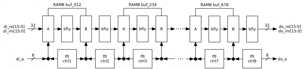
Fig.1 FFT256 diagram
3. [In Progress] FFT256 Verification.
NOTES:
- Do wires to BRAM36X36 and to MULT18X18 are shared? Can I use all 28 BRAMs and 28 MULTs in one design?
TODO:
- Check if the FFT256 results are correct.
- Write a correlation computation block.
- Write complex multiplication of 2 FFT256s (in order to get a cross-correlation spectrum)
- Add IFFT256 run for the multiplication result.
by Andrey Filippov
I’m considering using Xilinx high speed Serial I/O – 4 of the GTP in XC6SLX45T in CSG324 package (15mm x 15mm) to interface the sensor boards – it can be very attractive to be able to migrate to higher performance sensors from the current Aptina 5MPix ones. It would also enable higher bandwidth to the next version of the 10359 board – up to four of 3Gb/s channels, reduce EMI and enable longer cables.
The problem is that normally you need a large chip on the other (sensor) end capable of encoding data in a way compatible with the GTP – it would be an overkill for the simple CMOS sensor module. But it seems there is a way to use a tiny (5mm x 5mm) 3 – channel (plus clock – total 4) Texas Instruments SN65LVDS301 FlatLink(tm)3G that encodes 24 bit parallel data plus 3 sync signals into serial data. Maximal “pixel” rate – 65 MHz (not enough for MT9P031) but with additional register or better CPLD (like XC2C64A in CP56 6mm x 6mm package) it would be possible to double the pixel rate and add some scrambling to reduce disparity – not that critical as the data rate per pair would be only 480Mb/s. It seems that it would be possible to make GTP to accept that slow data rate, bond 4 channels (each still has to be able to recover it’s own clock) and use SN65LVDS301’s clock as a master in this bonding with a comma mask ox 10’b1111111111 and comma pattern of 10’b1111100000.
Most likely I’ll still use smaller XC6SLX25 (w/o “T”) first and use the bank that has GTP-s in 45T to connect the 30-pin parallel flex connector (compatible with the 10353 and the existent sensor boards) first, upgrading to high speed serial I/O in the next revision/model. that will be rather simple task as it will not require major PCB redesign – FPGA is side-by-side with the sensor connector, so those traces do not intersect with other ones.
by Oleg Dzhimiev
1. [Done] Add 1/256 after the last stage and check the simulation.
- Added a 1-bit right shift (1/2) after each “butterfly” – in the end it is 1/256 accumulated. This can be an early rounding. With 12 bits of color after all the sums in 8 stages the final value can be up to 20 bits wide. Only 16 bits are stored so the 1-bit right shift keeps the value within 12. Alternatively, a 4-bit right shift can be applied after every 4 stages.
2. [Done] Make a simple simulation with FFT256 and IFFT256.
- Made a testbench FFT256-IFFT256. The input and the output differ. Need to check more properly overflows in calculations and cosine tables.
- Corrected a mistake concerning two’s complement 8 bits expanding to 18 (just filling the upper part with the 7th bit(Hi)). Same for 16 bit values before 18×18 multiplication.
3. [In Progress] Optimize BRAM usage, the goal is 5 or 6 BRAMs & 8 MULTs (not sure for the input and output buffer)
- The plan is to use 4 BRAM32X32s and the output will be not buffered – the “butterfly” output needs to be delayed by 2 tacts then. And a specific writes and write order to input buffer will be needed.
TODO:
- Optimize BRAM usage.
- Add headers and commit to CVS.
- Write a correlation computation block.
- Set up memory controller for frames read/write.
- Integrate the correlation block to 10359’s firmware.
by Oleg Dzhimiev
1. Wrote a short manual on how to connect 10359 with 10353 and sensors: link
2. Almost finished coding FFT256 main module with no integration to 10359 code.
FFT is performed in 8 conveyor organized stages. Each stage is similar to as described here. So far each stage uses 1 BRAM and the 1 MULT18X18 (for the “butterfly”) + 1 BRAM for the input buffer – 9 BRAMs + 8 MULT18X18s. Plus other logic – 1 FFT256 uses 16% of FPGA resourses.
But, each ‘stage’ uses only a half of the BRAM (256 real and 256 imaginary). So it’s possible to optimize the module, the ways are:
- Currently the “butterfly” writes out Re & Im parts simultaneously using both (A and B) BRAM ports and only lower 512 cells. It is possible to use only one BRAM port doing writing and reading ‘Re’s and ‘Im’s sequentially and using lower 512 cells (as Re parts are calculated earlier) while another port can be used for other stage and access higher 512 cells.
- There are pauses between accesses to a BRAM – so stage-modules can be made working in turns.
Load time + Computation time + Readout time @10ns Clk ~ 2.5us + 8x5us + 2.5us = 45us.
But here it takes them 15us@25MHz to compute FFT256. They probably use only 1 tact for the “butterfly”. As I use only one MULT18X18 it takes 4 tacts to get the result:
4 x 128 x 10 ns ~ 5.12us per “butterfly”. With 1 tact & 4 MULTs it could be 1.28us and the overall FFT256 time 15us. But their clock is 4 times slower. How did they do that? Is it possibe to make a 4us FFT256 @96MHz?
With the 8-stage conveyor structure it speeds up by 8 times against non-conveyored computation. For a full resolution frame 2592×1944 with 128 bit overlap in a line it will take ~ (45us x (2592/128) x 1944) / 8 ~ 50us x 20 x 2000 / 8 = 0.25s or 4 fps
- Add 1/N after the last stage and check the simulation.
- Make a simple simulation with FFT256 and IFFT256.
- Optimize BRAM usage, the goal is 5 or 6 BRAMs & 8 MULTs (not sure for the input and output buffer)
- Can I get out of the 16-bit value border? Not cool if yes.