NC393 Development progress: Multichannel memory controller for the multi-sensor camera
Development of the NC393 camera has just passed an important milestone – we completed HDL code that constitutes the core of this new camera, tested most of the Zynq-specific features that were not available in the older Spartan-3 FPGA used in our current NC353 devices. Next development phase will involve porting some of the existing code that deals with sensor interfacing, gamma correction, histograms, color conversion and JPEG/JP4 compression – code that was tested in the thousands of cameras and many billions of processed images, including the applications listed in Wikipedia. New camera is designed primarily for the multisensor applications – up to four connected directly to the system board and more through the multiplexers as we currently do in Eyesis4π cameras. It is the memory controller that had to be redesigned completely, the sensor and compressor channels can reuse most of the existing code and just have 4 instances of the same modules instead of a single one. Starting early this year I’ve got an opportunity to put aside other projects and work full time on the new camera code.
Contents
FPGA features different from the previous Elphel cameras
The new features tested include I/O elements needed to implement DDR3 interface (described in the earlier posts) and communication between the ARM cores (PS – processing system) and the FPGA (PL – programmable logic). Zynq has multiple channels of communication based on AXI standards, 2 of the interface types are used in the current design:
MAXI_GP0 – general purpose memory-mapped interface controlled by the processors, convenient to write data to various registers inside the FPGA fabric that determine the operation of the device. Read channel of the interface allows CPU to get status information back from the PL. This interface is 32-bit wide and it is not intended for high bandwidth applications.
AXI_HP0 – high speed channel allowing 64-bit wide transfers between the system memory and the FPGA logic. Zynq offers 4 of such channels, current design uses one to implement a two-directional “bridge” between the system memory and the dedicated DDR3 device connected to the FPGA and used as an image/video buffer. Two of the remaining channels will be used to transfer compressed images to the system memory (to stream out and/or record to HDD/SSD), and one for SATA interface.
Other AXI channels that are not yet used in NC393 code include ACP (Accelerator Coherency Port) that has the same bandwidth as the AXI_HP, but “sees” the memory the same way as the processors do (through the same cache levels), this port is intended as its name suggests for the “accelerators” – programmed logic tightly coupled with the CPU, where the latency is critical but the amount of data transferred is relatively small, so it will not disturb the normal cache usage by the processors.
Implementation of the HDL code that interacts with these AXI ports took more time than it should, partly because the Zynq manufacturer does not provide HDL code for simulation, only proprietary encrypted modules are available – modules that are useless for our preferred Free Software tools. When I tried to simulate AXI interfaces I only got the output from the following statement:
$display("Warning on instance %m : The Zynq-7000 All Programmable SoC does not have a simulation model. Behavioral simulation of Zynq-7000 (e.g. Zynq PS7 block) is not supported in any simulator. Please use the AXI BFM simulation model to verify the AXI transactions.");
We had to implement both the synthesizable HDL modules for our product and the simulation code for MAXI_GP and AXI_HP missing from the software distribution. This code definitely has limitations compared to the proprietary encrypted one – we implemented only the features needed in our design (for AXI_HP it does not provide 32-bit bus functionality). Nevertheless it seems to work for our application and is now available under GNU GPLv3 license for others to use as a part of x393 project at GiHub.
Custom memory controller
External memory controller is a rather intimate part of the system design and I do not believe it is possible to create an efficient one-size-fits-all code. Yes, Xilinx offers MIG IP that can be inserted into your custom design, but we need more control over what is going on inside it, the earlier post “DDR3 Memory Interface on Xilinx Zynq SOC – Free Software Compatible” describes the physical layer (PHY) of the implementation. Dynamic RAM devices impose multiple access restrictions, and the general purpose memory controller essentially tries to hide these details from the processes that use the memory, while keeping the data rate as close as possible to the theoretically available (clock frequency multiplied by bus width multiplied by two for DDR devices).
Some of the main specifics of the dynamic RAM devises are:
- Memory is page-oriented, access within the same page is fast, but opening/closing pages (“activate” and “precharge” terms are used in the device manuals) is slow
- Data transfer happens in multi-word “bursts”, DDR3 devices have normal bursts of 8 words (width depends on the memory organization) and short ones of 4 bursts, but short bursts use the same time as the 8-long ones so they do not offer advantage when transferring large amount of data. For our application we can consider memory device to be 128-bit (8*16 bits) wide
- Memory array is divided into “banks” (DDR3 has 8 of them), and transfers to/from one bank can take place with simultaneous activation/precharging of other one(s) as these operations do not use the data bus.
These features provide a clue – how to get a high average bandwidth. Basically there are 2 strategies:
- Consolidate multiple accesses to the same page. In the simplest form (common for the camera designs) write consecutive memory locations (like fill memory with the scan-line data from the sensor). With 16-bit wide memory it is possible to transfer up to 2048 bytes at the full memory bandwidth with just one “activate” in the beginning and one “precharge” (or auto-precharge) in the end.
- Design the memory addressing in such a way, that translation of the linear address to physical bank, page number (“row address” in DRAM terminology) and in-page address (“column address”) makes it likely to simultaneously operate multiple banks.
While the first clue is easy to follow, the second one is not. Depending on the particular clock speed/timing parameters, you may need 3-5 banks to interleave to provide full data bandwidth utilization, something rather difficult to achieve for random data access without making special assumptions about the nature of the application data.
Camera deals mostly with the 2-d data arrays and majority of scenarios use either sequential (scan-line ordered) access or depend on 2-d locality of the pixels (compression, de-warping, correlation, filtering, and more). This mode can use tiled access and read/write small rectangular pixel areas as atomic operations. Contrary to the general processing memory, latency is not usually critical for the image memory, access patterns are predictable and can be pre-optimized in advance, not at the run time during memory access.
This allows to optimize a custom memory controller dedicated to image acquisition, processing and compression, and in our case support multiple image sensors operating in parallel. Particular application may include optical image-guided UAVs and other robotic devices.
Memory mapping and access types
Mapping of the 2-d imaging objects to the DRAM memory addresses targets both sequential and tiled accesses. Each image scan line uses a single bank address (0..7) and increasing column addresses (2048 bytes or 128 bursts), then row addresses. Each group of 8 lines share the same row/column addresses and have individual banks for each row as shown on Fig.1.
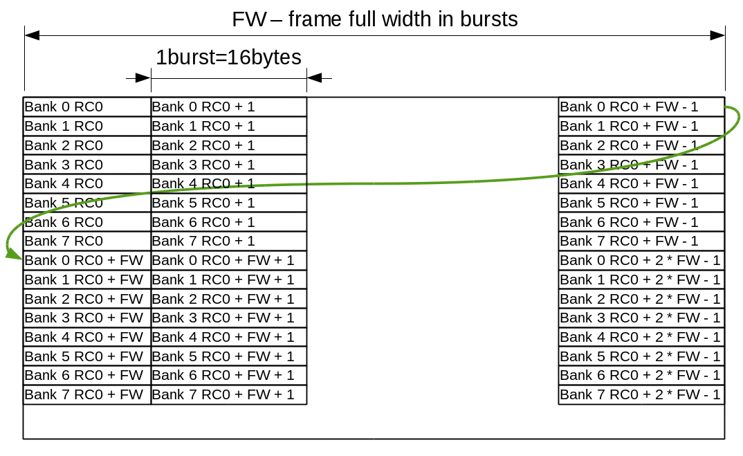
Figure 1. Memory layout for 2-d image objects
Atomic memory accesses are currently limited to ¼ of the 4KB BRAM memory blocks available in Xilinx Zynq FPGA part, that makes 64 bursts or ½ of the memory page. Crossing page boundary during sequential access requires precharge and activation of the different memory pages in the same bank, so while the code can split accesses automatically it is beneficial to align the full frame width to the multiple of the 64 bursts (1024 8-bit or 512 of 16-bit pixels).
Scanline frame access
Memory controller provides application modules with a scanline windowed access to the image frames defined by the memory start address and the full (possibly padded) frame width, measured in 16-byte bursts. Access window is defined by conventional X0, Y0, width (in bursts) and height (in lines/pixels).
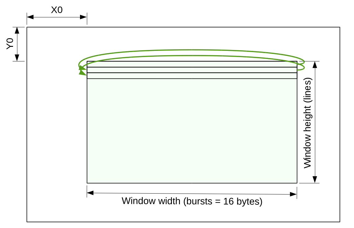
Figure 2 Access window in scanline mode
Scanline access module splits the requested window into a sequence of up to 64-burst data transfers, generates “page ready”, “frame ready” signals to application module, accepts “frame start”, “next page” signals. It also supports inter-channel synchronization by providing “next line number” output and “suspend” input. External module can compare last line number acquired from the sensor input channel and suspend compressor/image processing module, providing low-latency video.
Tiled frame access
Many image processing and compression algorithms consume or generate 2-d blocks(tiles) of data. Some applications require overlapping tiles, including regular JPEG compression of color images. While compression algorithm itself uses non-overlapping 8×8 pixel blocks (16×16 macroblocks for 4:2:0 mode), extra pixels around the blocks are needed for Bayer-to-YCbCr conversion that is convenient to implement right in front of the compressor where the data is already available in 2d format, not in scanline order as it comes out of the sensor.
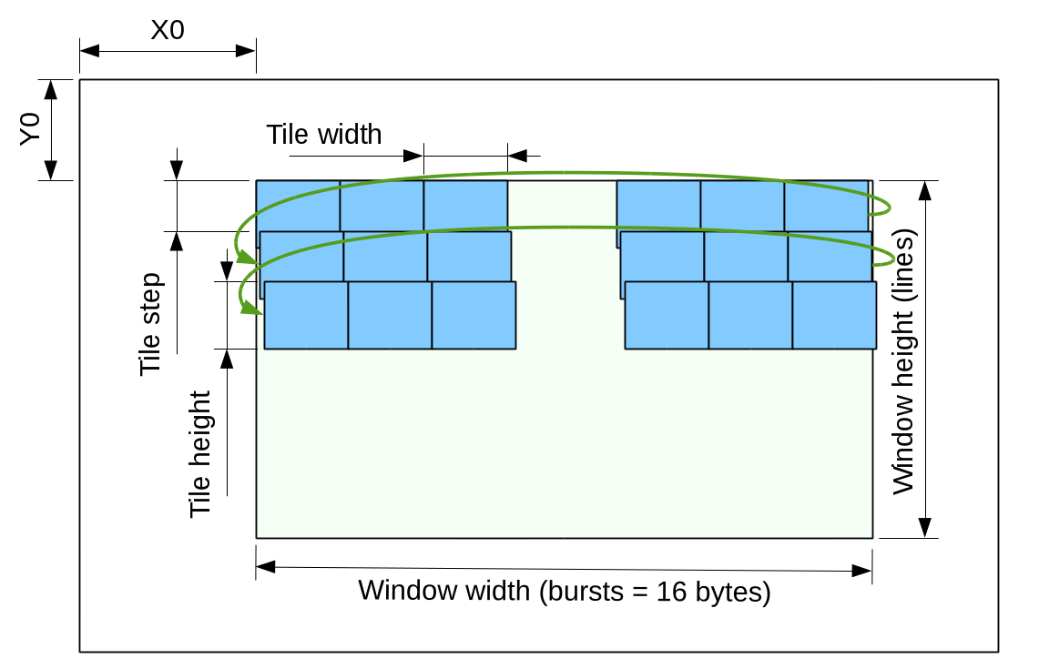
Figure 3 Access window in tiled mode
Tile overlap is needed both horizontally and vertically, but horizontal overlap is easy to implement in the application module just by using already buffered (in FPGA BlockRAM) data from the previous tile, while vertical overlap would need buffering the whole width of the sensor that would be not scalable for high resolution sensors and would require extra BlockRAM modules in the fabric. This is why the memory controller module provides only vertical tile overlap, accepting 3 byte-wide (width is limited by the total “area” of 64 bursts in a tile) parameters – tile width, tile height and tile step in addition to X0, Y0, window width and window height.
Tile internal structure
Memory controller provides support for the 2 types of tiles. First type (Tile16) maps data to the sequence of bursts as vertical columns, each burst representing horizontal row of 16 (8-bpp mode) or 8 (16bpp mode) pixels.
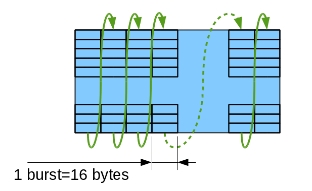 Figure 4a: Tile16 – tile with 1 burst-wide columns |
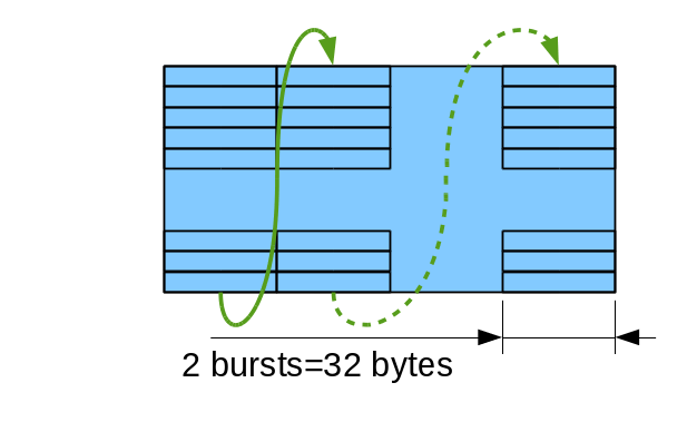 Figure 4b: Tile32 – tile with 2 burst-wide columns |
Columns are traversed up to down, then left to write as shown on Fig. 4a. Due to memory timing restrictions this mode allows only some values for the tile height (0,6 and 7 modulo 8). Tile32 allows more variants for the tile height as there is more clock cycles between re-opening different page for the same bank, it can be (0,3,4,5,6,7 modulo 8). All tiles with the height of less than or equal to 8 are valid as it is possible to keep all banks open between columns of a tile, all heights are valid for the single-column tiles too. Single-column tile32 of maximal size (64 bursts) corresponds to a square area of 32×32 pixels in 8 bits per pixel mode.
NC393 HDL code and the memory controller implementation
Elphel camera code is built around the 16-channel DDR3 memory controller and at this stage the only modules that are not part of this controller are command and status distribution networks, system memory to external memory bridge over AXI_HP and temporary test modules to test controller functionality.
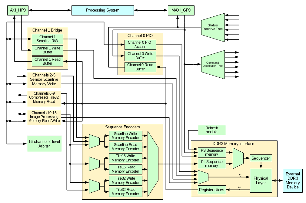
Figure 5. Memory controller block diagram
Command and status networks
Command distribution tree is designed to write data to various memory-mapped registers distributed over the whole design. All these registers are write-only (readback is optionally provided by a separate Block RAM-based module), so data paths can accommodate any number of register slices if needed to meet timing. This bus is a light-weight to minimize required routing resources of the FPGA, it requires only 9 data signals (9 address/data and a strobe) and can deliver 0 to 32 bits of data (configured by parameters at the destination module) sent over 1 to 6 clock cycles. Command distribution tree accepts commands from the software over the MAXI_GP0 or from a PL sequencer driven by the frame synchronization signals from the sensors – it will be ported from the current NC353 camera HDL code.
Status receive tree supplements the command tree and provides processing system with a feedback data from the distributed over the FPGA fabric modules. It includes a 256×32 register file available for PS read access with zero latency and a unidirectional tree of light-weight (10 signals) network that also includes multiplexers and status transmitters. Multiplexers route the messages (up to 6 clock cycles long depending on a payload) to the terminating register file. Status transmitters (controlled through the command distribution network) provide means to synchronize responses to the PS requests using 6-bit IDs, they send up to 26-bit status information either in response to a command or automatically when the input data changes.
Memory interface
Memory interface is forked from an earlier eddr3 project (there are some important bug fixes). In addition to the physical layer components it includes sequencer that generates address and control signals for memory device access following the program data prepared in advance. This sequence programs come from one of the two sources – PS Sequence Memory written under the software control and PL Sequence Memory filled in by one one of the Sequence encoders just before (during previous memory transaction) the execution. Both memories are made of 4KB Block RAM modules. PS sequences are used for memory refresh access instructions, memory initialization and calibration, any other pre-programmed memory operations that need to be executed following specific timing.
Memory interface is configurable with Verilog `define macros and can interface up to 16 concurrent channels, each being read-only, write-only or bidirectional. Each channel is supposed to have a 4KB block RAM buffer (or two of them for bidirectional channels) configured in SDP (simple dual port) mode with 64-bit wide input (for memory read) or 64-bit output (for memory write). Memory interface also provides channels with clock and control signals for the memory side of the buffers, other side of these dual-port buffers is under channel logic control, it may be clocked by a different source. Two layers of registers may be inserted in both input (16:1) multiplexer path and output distribution of the 64-bit wide data buses that may need routing to different parts of the device.
Channel buffers are based on 4KB block RAM modules, each split into 4 of 1KB pages, making them suitable for up to 64 of 16-byte bursts transfers. Of the four pages one (in some overlapping tiles applications – two) is in use by the channel logic (being consumed or generated), another is used by the transfer to/from the DRAM memory, and the remaining ones provide needed buffering when memory is in use by the other channels.
Channel arbiter
16-channel arbiter accepts two levels of urgency (“want” and “need” signals) from the channel controllers. In most cases memory read channels generate “need” if there is at least one empty buffer page and the channel will need it later (not the last pages in a frame), “need” is generated when the channel is consuming the last available page. Similarly for the memory write channels – “want” is generated when there is at least one completed page, “need” – when there is no empty pages left. Channels that can wait for the data can skip raising the “need” signal leaving more resources to other channels that are tied to constant data rate data (such as inputs from the sensors).
In addition to the two levels of urgency (channels with ”need” requests are served before “want” ones compete) arbiter provides channel priorities. Each channel has associated counter that increments at each event (new request or request grant), taking care of the simultaneous requests by static priority by channel number. The channel having highest counter value wins, receives “grant” signal and that channel counter is reset to the specified channel priority value, so priority 0 makes that channel to wait maximal time.
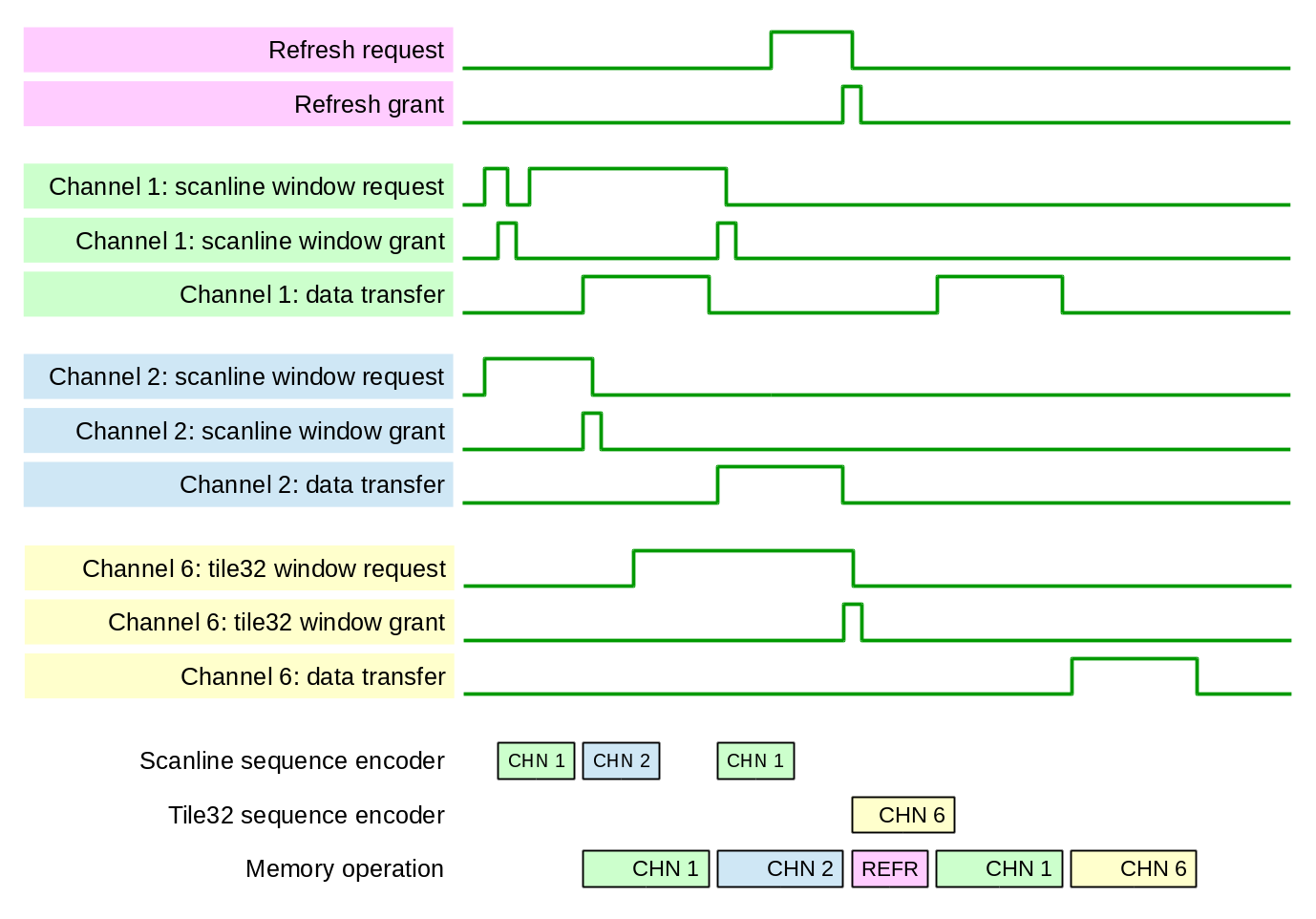
Figure 6. Memory access arbitration and timing
Sequence generation takes less time than the actual memory access, and channel arbitration happens when the previous sequence data is sent for execution. Fig. 6 shows that channel 2 sequence is started to be transferred to the PL Sequence Memory as soon as the memory interface starts to execute sequence for channel 1.
There is an additional arbitration just before starting to execute a sequence – if refresh module (it does not need to transfer sequence data as it is already in the PS Sequence Memory) generates “want” or “need” request, it competes against the already granted channel that has the sequence ready to be executed – Fig. 6 shows how REFR sequence passes the CHN1 that is ready to be executed. The sequence FIFO in PL Sequence Memory allows only one sequence to be buffered. This limit is imposed to reduce waiting for service of the urgent (“need”) requests while not using a more complicated mechanism that would allow such requests to pass other channel non-urgent (“want”) requests in the sequence memory FIFO. It is still a possibility for the future improvements to allow efficient execution of significantly different size memory transfers.
Sequence Encoders
Sequence encoders are shared between the channels – the channel that wins the arbitration is granted to generate a memory access sequence. Currently there are 6 of such modules that generated scanline read, tile16 and tile32 (see Fig. 4a-b) and similar for memory writes. These modules accept address and size parameters from the window access controllers and use HDL-encoded templates to generate control sequence for the next memory access operation.
Channel window access controllers
Window access controllers implement access to selected rectangular areas inside the image frame. There are two types currently available – scanline access (Fig. 2) and tiled access (Fig.3). Distinction between read and write modes, and between tile16 and tile32 modes are passed as run-time parameters. They are used later to select the specific sequence encoder each time the request is granted by the arbiter. These modules require individual instances for each channel that uses them as they have to keep track of the related channel buffer, tile location and other module state variables.
Additional controllers will be developed for other types of accesses when needed by the image processing algorithms that may need other types of memory accesses. Example application may be a distortion correction procedure where either input or output use tiles that are not defined by a regular grid).
Memory access channels
Channel 0 is designed for programmable access to the memory. It uses PS Sequence Memory written through MAXI_GP0 under the software control. It has both read and write buffers for operations that involve data transfer, it is used for memory initialization and calibration/training, it can also be used to test other access sequences without re-generation of the bitstream.
Channel 1 implements a fast bi-directional bridge between the system memory and the dedicated image memory. On the system side it uses AXI_HP0 port in 64-bit mode, on the image memory side it implements a scanline window access It is possible to either fill the selected window in the image memory with the consecutive data from the system memory, or read image memory window to a linear array in the system memory.
Channels 2-5 will be used to record data from the four sensor ports, currently one channel is connected to 2 buffers connected to the MAXI_GP0 interface for testing scanline windowed memory access.
Channels 6-9 will be used in tile32 mode to read 2d data for image compression. Temporary implementation uses 2 channels connected to MAXI_GP0 read/write for testing purposes.
Remaining six channels may be used for application-specific image processing.
Software tools used
The list of the tools used for this project is the same as listed for the earlier eddr3 project. The only difference is that now it is Eclipse Luna instead of Kepler, and some bugs in VDT plugin are fixed – bugs that revealed themselves while this plugin was being used with gradually growing code base.
The x393 project code itself is available under GNU GPLv3 Free Software license, does not depend on any undocumented or encrypted “IP” modules and can be simulated with the Free Software tools. Project configuration files allow importing it to Eclipse IDE when VDT plugin is installed.
Leave a Reply