June 29, 2009
by Andrey Filippov
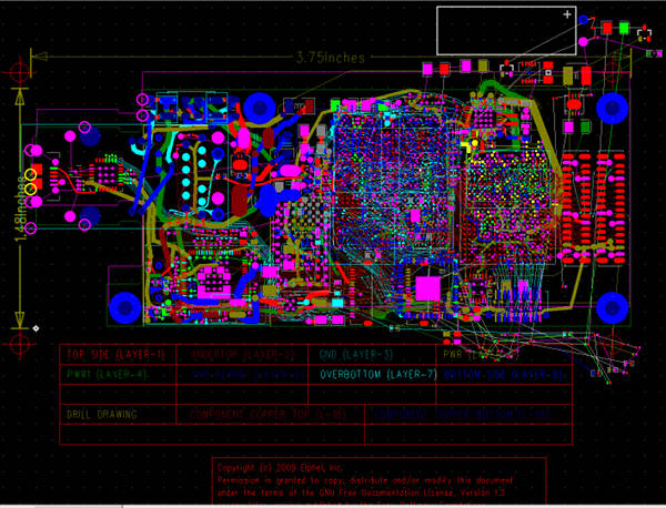
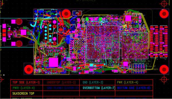
After finishing the 10373 layout I did not feel satisfied – some valuable parts of the PCB were left wasted. When I was just starting this project I new I’ll have to use more layers (now 8, previous designs – 4), smaller traces (0.075 mm – down from 0.1mm) and use buried and blind vias that I never did before. And I still was not sure if everything will fit on the same board size, I even had a plan B for the system memory – use just one x16 chip and have lower bandwidth, but both chips did fit nicely (they are visible as large vertical rectangles just above the center of the board). And when I just started placement, I noticed that several hundred of huge 0402 resistors and capacitors will not actually fit around the chip with 0.4mm distnace between the pads. Each such resitor is longer than a millimiter, so I changed most of them (few do not exist in small package) to 0201 – that was better, just 0.6mm by 0.3mm. End everything did fit and some extra remained so I’m trying to put more of the useful components.
So I broke the layout, renamed the board to rev “A” (even as rev “0” was never build) and added few more connectors, ICs and other components and now I’m working on making the increased number of parts fit (some are still around the board, not yet placed). That huge supercapaitor on top (used for clock/calendar backup instead of a battery) will be placed over other components so it does not need that much empty space.
It will take me some time to fit everything, but it seems to be possible. And then the board will be really packed with no space wasted. And camera board – get more functionality even when no extension board will be installed.
Andrey

June 23, 2009
by Oleg Dzhimiev
1. [In Progress] “Verification of everything”
Images below show the results of tests on 10359 board. Fig.2 represents the displacement map multiplied by 128 – {dires_data_out[4:0],7’b0}. The correct resulting image should be black as the maximum of the correlation function must be in 0. Checked the results in simulation – they are the same. Verifying.

Fig. 1 Input image, same image comes from the 2nd channel (Left=Right).

Fig. 2. Result image (incorrect)
June 22, 2009
by Andrey Filippov
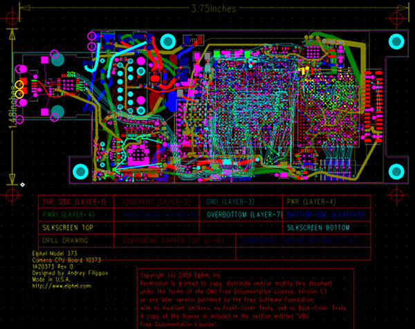
After finishing the PCB layout of the 10373 board I noticed that it is very easy to add a second sensor board connector.
First of all – there is room for that connector – space wasted between the two tabs with mounting holes that we added at the request of our customer. And the connector nicely fits there.
Then – the bank 0 of the Spartan 6 FPGA has enough pins for 2 sensor ports (each port uses 22 I/O lines).
The 10373 board is expected to have 3-4 times higher processing speed than 10353 so using it with the current sensor boards would keep it under-loaded. For the newer (and faster) sensors I plan to use high speed serial transceivers of the Spartan chips as I wrote earlier, but the first revision will be compatible with the older sensors.
That second connector would cost just the price of the connector as I use free so far space on the board and unused pins on the FPGA. It can be used in multiple ways, such as:
1 – stereo cameras. It will be possible to incorporate code Oleg is working on now for automatic processing of the 3-d information – i.e. for autonomous vehicles. And having higher bandwidth of the system and network it will be possible to stream or record both of the stereo channels at the full resolution/frame rate sensor is capable of – it could be used for stereo cinema applications.
2 – panoramic applications with fewer number of complete camera modules, fewer network ports than needed currently when the 353 cameras are used.
3 – Day/night cameras with both color (with IR cutoff filter) and monochrome (without filter) sensors connected at the same time.
Andrey
Now it looks like this:

June 16, 2009
by Oleg Dzhimiev
1. [Done] Finish with the “full_pages_in_buffer“. Made more convenient to me and corrected the error I had done before (double write request from channel).
2. [In Progress] Verification of everything.
Currently instead of black frames I get different ones (apparently, something’s wrong: black vertical lines after each 1024 pixels) – checking the simulation:

Fig. 1 Test image, size 2592×1940
TODO:
1. Verification.
2. I also didn’t implemented multiplication on the Hamming function before performing the FFTs.
June 15, 2009
by Andrey Filippov
I do not know why search engines love this 8-year old page – current camera model is 393. It’s PCB layout is also available in both Gerber and PDF form on this wiki page.
I’m working now on the 10373 PCB layout – there will be some minor cleanup and double-checking all the new components used, their mechanical dimensions and pinouts, but so far I was able to fit all the components to the same size PCB and route all the traces. Sure I had to use more layers – there are 8 now, including 4 dedicated to ground and power planes, there are now blind laser microvias between the the outer layers and the next ones, some buried vias and reduced traces widths.
And there is even some room left on the board – something to be added later in the next revision.
Andrey

June 1, 2009
by Oleg Dzhimiev
1. [Done] Simulation of data path of Cross-Correlation (C-C) module.
2. [Done] Integration of the C-C block to x359.
3. [In Progress] Simulation of the C-C and x359 as a whole.
3.a. [Done] Set up memory controller.
- Write length is set to 64(8×8) words.
- Fixed image size to 2592×1944.
- C-C block is set to work with 512 words, reading out 256 word at a time with overlapping – 3 256-word reads till another command to the C-C block.
3.b. [Done] Simulate for 1 write and 1 read channels. Here there are no competetive requests from 2 write channels.
3.c. [In Progress] Simulate for 2 write and 2 read channels.
- Fixed reg “full_pages_in_buffer” correct work. It was commented earlier by me as I used only one channel at a time to access SDRAM.
- For write channels – changed reg “full_pages_in_buffer” size to 32 (page size is 64). And if it reaches the maximum then a aditional BRAM is neaded.
TODO:
1. Finish with the “full_pages_in_buffer“.
2. Make an x359.bit and check the work with the whole frame.
3. I also didn’t implemented multiplication on the Hamming function before performing the FFTs.
