FPGA to DDR3 memory interface: step-by-step timing calibration and set up
Working with the DDR3 Memory interface I was not able to avoid the temptation to investigate more the very useful feature of the modern FPGA devices – individually programmed input/output delay elements on all (or at least many) of its pins. This is needed to both prepare to increase the memory clock frequency and to be able to individually adjust the timing on other pads, such as the sensor ports, especially when switching from the parallel to high speed serial interface of the modern image sensors.
Xilinx Zynq device we are using has both input and output delays on all low-voltage pins used for the memory interface in the camera, but only input ones on the higher voltage range I/O banks. Luckily enough image sensors connected to these banks need just that – data rate to the sensors is much lower than the rate of the data they generate and send to the FPGA.
Contents
- 1 Adjusting memory timing with Python code
- 2 Delay elements in the memory interface
- 3 Measuring delays in the signal paths and setting memory interface timing
- 3.1 Step 1 : Finding valid command/address delays for each clock phase setting
- 3.2 Step 2: Measuring individual delays for command (RAS,CAS,WE) lines
- 3.3 Step 3: Write levelling – finding the optimal DQS output delays for clock phase
- 3.4 Step 4: Fixed pattern measurements
- 3.5 Step 5: Measuring DQS input delay vs. clock phase
- 3.6 Step 6: DQ to DQS output delays measurements
- 3.7 Step 7: Measuring individual output delays for all address and bank lines
- 3.8 Step 8: Selecting valid parameter combinations for readout and write modes
- 4 Model and parameters of the input/output delay elements
- 5 Features I would like to see improved in the future Xilinx devices
Adjusting memory timing with Python code
Adjustment of the optimal pin delays for the memory interface can be done in several ways, and many applications require that it should be either all implemented in hardware or use very limited CPU resources – that is the case when the memory to be set up is the main system memory and so CPU can not use it. On the other hand when the memory is connected to the FPGA part of the system that is already running with full software capabilities it is possible to use more elaborate algorithms.
I call it for myself “the Apple ][ principle” – do not use extra hardware for what can be done in software. In the case of the delay calibration for the memory interface it should be possible to use a reasonable model of the delay elements, perform measurements and calculate the parameters of such model, and finally calculate the optimal settings for each programmable component. Performing full measurements and performing parameter fitting can be a computationally intensive procedure (current Python implementation runs 10 minutes) but calculating the optimal settings from the parameters is very simple and fast. It is also reasonable to expect that individual parameters have simple dependence on the temperature so it will be easy to adjust parameters to the varying system temperature. Another benefit of such approach that it can use delay elements with even non-monotonic performance (that is sometimes in case when using FINEDELAY elements) and finally – the internal parameters of the delay elements do not depend on the clock frequency, so parameters can be measured at lower clock frequency and then settings can be re-calculated for the higher one. Adjusting timing parameters at the target frequency can be more difficult as there can be much smaller windows of the combination of the parameters that allow memory device to operate, it may be not possible to probe marginal values of some delays (to calculate the optimal center value) as it may violate other timing parameters.
The procedure described below can be used to measure the delay parameters of the memory interface and find the optimal combinations of the settings requiring no manual adjustments of the initial values. The software is written in Python and is a part of the Elphel GitHub repository x393 as x393/py393 PyDev project.
The Python code includes a module that can parse Verilog header files with parameter definitions so all the changes in the HDL code are automatically applied to the Python program, running the program on the target hardware generates updated values of the delay settings as a Verilog file, so these measured values can be used in simulation. This program is of course designed to run on the target platform, but most of the processing can be tested on a host computer – the project repository contains a set of measured data as a Python pickle file that can be loaded in the program with a command “load_mcntrl dbg/x393_mcntrl.pickle”. Program can run automatically using the command file provided through the arguments, it also supports interactive mode. Most of the functions defined in the program modules are exposed to the program CLI, so it is possible to launch them, get basic usage help. Same is true for the Verilog parameters and macro defines – they are available for searching and it is possible to view their values.
Delay elements in the memory interface
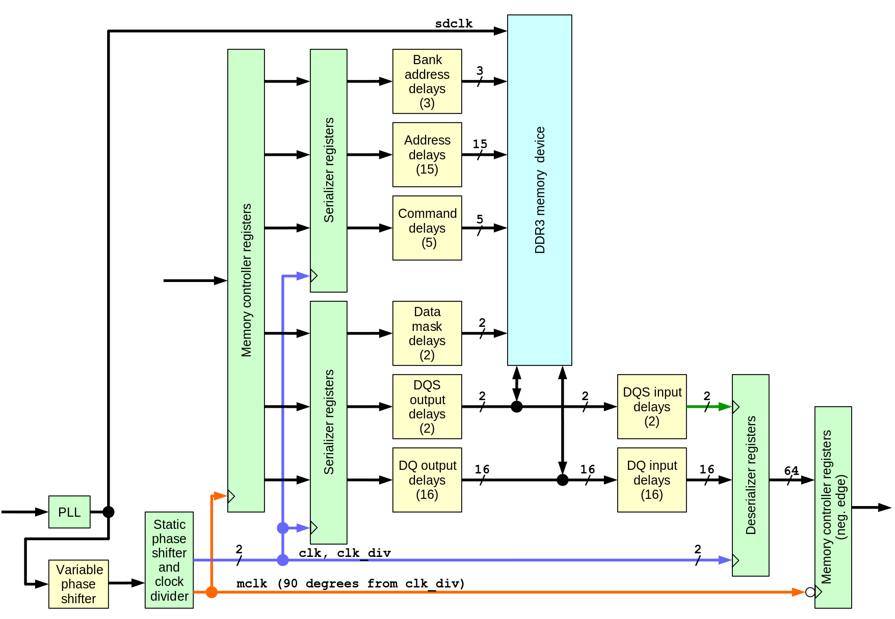
Fig.1 Memory interface diagram showing signal paths and delays
There are total 61 programmable delays and a programmable phase shifter as a part of the clock management circuitry. Of these delays 57 are currently controlled – data mask signals are not used in this application (when needed they can be adjusted by the similar procedure as DQ output delays), ODT signal has more relaxed timing and the CKE (clock enable) is not combined with the other signals. There are 3 clock signals generated by the same clock management module with statically programmed delays: clk (same frequency as the memory clock), clk_div (half memory frequency) and mclk – also half frequency, but with 90 degree phase shift with respect to clk_div, it is driving the memory controller logic. Full list of the clock signals and their description is provided in the project.
Variable phase shifter (with the current 400 Mhz memory clock it has 112 steps per full clock period) is essentially providing variable phase clock driving the memory device, but to avoid dependence on the memory internal PLL circuitry, memory is driven by the non-adjusted clock, and programmed phase shift is applied to all other clock signals instead.
Address/control signals and data to be written to the memory device originate in the registers and Block RAM of the controller running at mclk global clock, then they go through serializers (OSERDESE2 for synthesis, OSERDESE1 for simulation to avoid undisclosed code modules). Serializers use two clocks and in this design the slower clk_div is ¾ of the mclk period later than mclk itself to guarantee positive setup time when crossing the clock boundary. Serializers for data, data mask and DQS strobes operate in DDR mode, while the ones for address and command signals use single data rate mode. Each of this signals pass through individual 32-tap delay with nominal 78 ps/step, followed by a a 5-tap fine delay element (ODELAYE2_FINEDELAY) and then go to the external memory device.
On the way back the data read from the memory and the read strobes (one per each data byte) pass through IDELAYE2_FINEDELAY elements and then strobes pass through BUFIO clock buffers that drive input clock ports of the deserializers ( ISERDESE2 for synthesis, ISERDESE1 for simulation), while the same (as used for the output serializers) clk and clk_div drive the system-synchronous ports. When crossing clock boundary to the mclk registers that receive data from the deserializers use the falling edge of mclk and there is again ¾ of mclk period to guarantee positive setup time.
The delay measurement procedure involves varying the delay that has uniform phase shift step (1/112 memory clock period) and adjustment of the variable “analog” pin delays that have some uncertainty: constant shift, scale (delay per step) and non-linearity. The measurement steps that require writing data to the memory and reading it back, and so depending on the periodic memory refresh, the automatic refresh is temporarily turned off when the clock phase and command delays are modified.
Measuring delays in the signal paths and setting memory interface timing
Step 1 : Finding valid command/address delays for each clock phase setting
The first thing to do to be able to operate the memory is to find the address/command line delay that is safe to use with each clock phase and/or find what values of the phase shift are valid. The address and command signals use single data rate (sampled at the leading edge of the clock by the memory device) so it is easier to satisfy the setup/hold requirements than for the data. DDR3 devices provide a special “write levelling” mode of operation that requires only clock, address/command lines and DQS output strobes providing result on the data bus. At this stage timing of the read data is not critical as the data data stay the same for the same DQS timing, and it is either 0x00 or 0x01 in each of the data bytes.
It is possible to try reading data in this mode (reading multiple data words and discarding groups of first and last one no remove dependence of read data timing) and if the result is neither 0x00 nor 0x01 then reset the memory, change the command delay (or phase) by say ¼ of the clock period, and start over again. If the result matches the write levelling pattern it is possible to find the marginal value value of the address delay by varying delay of address bit 7 when writing the Mode Register 1 (MR1) – this bit sets the write levelling mode, if it was 0 then the data bus will remain in high impedance state.
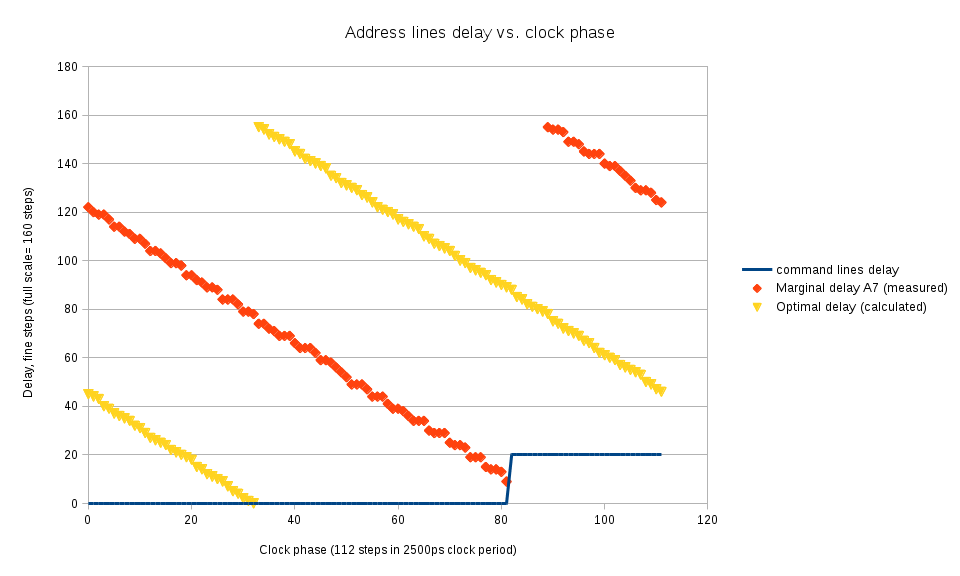
Fig.2 Finding the command/address lines delay for each clock phase
Memory controller drives address lines in “lazy” mode leaving them unchanged when they are not needed (during inactive NOP commands) so it is easier to check if A[7] low → high transition happens too late. Additionally the tested write levelling command have to be preceded by some other command with A[7] at low level.
Figure 2 shows the process of scanning over phases and finding the longest delay on A[7] line that still turns on the write levelling mode (shown with red diamonds). Command line delays are kept at zero until at phase 82 the delay on A[7] line becomes smaller than a preset limit (command lines are almost too late themselves), at this phase the command line delay is increased so the command is recognized in the next clock cycle and so the marginal value of A[7] is also increased by the full clock period. With the current settings the full delay range is almost exactly equal to the clock period, this will not be the case at higher memory clock rates (delays will cover more than a period) or increasing the delay calibration clock rate from 200 MHz to 300 MHz (delays will cover les than a period). On the Figure 2 there is a small gap (to phase=86) when the marginal delay for A[7] can not be measured as it would exceed the maximal delay value available in OSERDESE2 element.
Yellow triangles show the optimal values for the A[7] delay calculated by applying linear interpolation to the marginal values and shifting the result horizontally by ½ of the clock period (56 phase steps).
At this preliminary stage optimal command/address delays are assumed to be the same as for the A[7] – they are connected to the same I/O bank. Later it will be possible to optimize each signal delay individually, when switching to the higher frequency the relative differences between lines can be assumed the be the same and can be applied accordingly.
During the next stages of the delay measurement the command and address lines delay values are all set whenever the clock phase is changed.
Step 2: Measuring individual delays for command (RAS,CAS,WE) lines
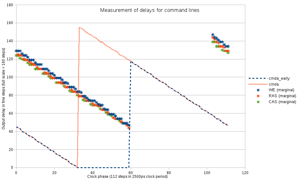
Fig.3 Command lines delays measurement
When the approximate value for the optimal delay for the address/command lines is known it is possible to individually calibrate delay for the command lines. The mode register set command involves high (inactive) to low (active) state on all 3 of them, so it is possible to probe turning on the write levelling mode when 2 of the the 3 command lines (and all the bank and address lines) are set with the optimal values, while the delay on the remaining command line is varied. Sometimes this procedure leads to the memory entering undefined/non-operational state (write levelling pattern is not detected even after restoring known-good delay values), when such condition is detected, the program resets and re-initializes the memory device.
To increase the range of the usable phases the other command/address lines are kept at delay=0 while there still is a safe margin of the setup time with respect to memory clock (from phase = 32 to 60 on Fig. 3)
Step 3: Write levelling – finding the optimal DQS output delays for clock phase
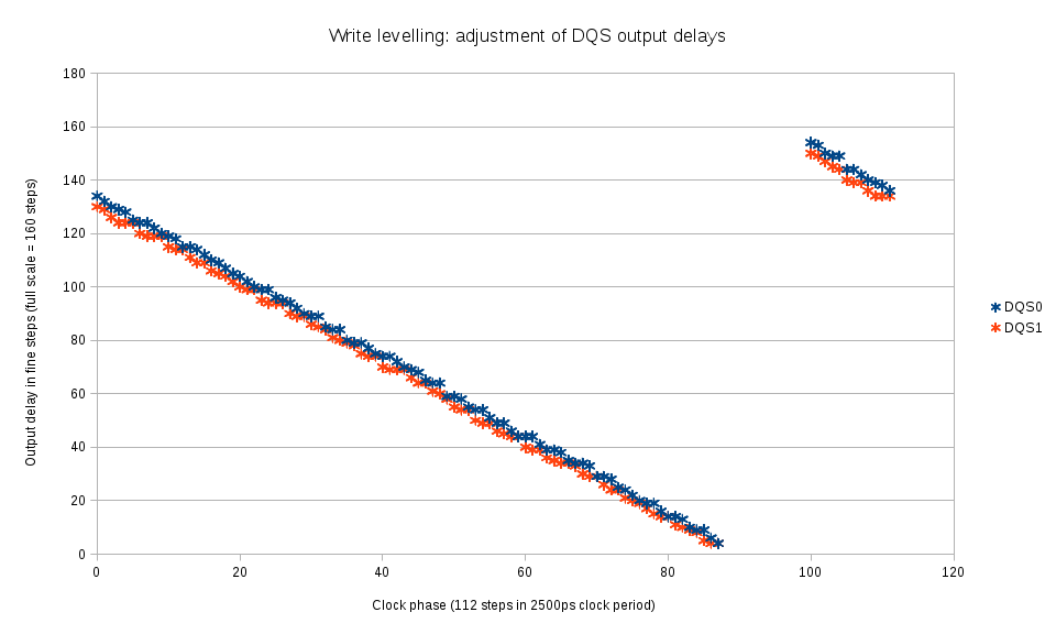
Fig.4 DQS output delay measurement with write levelling mode
This special mode of DDR3 devices operation is intended to adjust the DQS signal generated by the controller to the clock as seen by the memory device, it measures clock value at the leading edge of the DQS signals and replies with either 0x00 (clock was low) or 0x01 (clock was high) on each data byte of DQ signals.
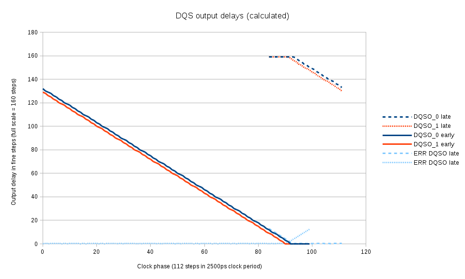
Fig.5 Calculated optimal DQS output delays for each clock phase
The clock phase is scanned over the full period and for each phase the marginal (switching from 0x00 to 0x01) DQS output delay is measured for each of the byte lanes. This procedure directly results in the optimal values of the DQS output delay values, there is no need to shift them by a half-period. Fig. 5 shows the calculated by linear interpolation values of the DQS output delays for each phase. To increase the range of DQ vs. DQS delay measurements, the DQS output signals are allowed to slightly deviate from the optimal – Fig. 5 shows “early” and “late” branches and the amount of deviation.
The similar calculation is performed later once more time when additional data from co-measurement of DQ output delays and DQS output delays becomes available. At that stage it is possible to account for non-uniform fine delay steps of DQS output lines.
Step 4: Fixed pattern measurements
DDR3 memory devices have another special operational mode intended for timing set up that does not depend on actual data being written to the memory or read back. This is reading a predefined pattern from the device, currently only one pattern is defined – it is just alternating 0-1-0-1… on each of the data lines simultaneously. In this step the 11 of the 8-word bursts are read from the memory, then only the middle 8 bursts are processed, so there is no dependence on the (yet) wrong timing settings that result in the wrong synchronization of the data bursts. That provides 64 data words, half being in even (starting from 0) positions that are supposed to be zeros, and half in odd ones (should read all 1-s), and then total number of ones is calculated for each data bit for odd and even slots – 16 pairs of numbers in the range of zero to 32. These results depend on the difference between delays in the data and data strobe signal paths and allow detection of 4 different events in each data line: alignment of the leading edge on the DQ line to the leading edge of the DQS signal (as seen at the de-serializer inputs), trailing edge of the DQ to leading one of DQS and the same leading and trailing DQ to the trailing DQS. They are measured as transitions from 0 to 1 and from 1 to zero separately for even and odd data samples.
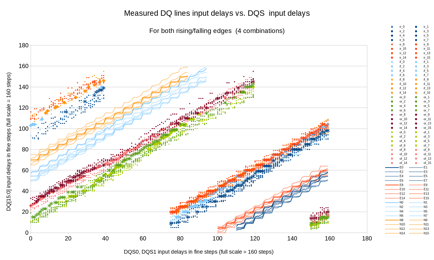
Fig.6 Measured (marginal) and calculated (optimal) DQ input delays vs. DQS input delays
Most results have 0 or 32 values (all data words are read 0 or 1), but some provide intermediate “analog” results when corresponding words are read differently, depending on some uncontrolled factors. Later processing assumes that the difference from the middle value (16) is proportional to the difference between the measured (by the settings) delay value and the actual one. Additionally if the number of such analog samples is sufficient, it is possible to process only them and discard “binary” (all 0-s/all 1-s transitions).
This measurement can be made with any clock phase setting. Even as normally there is a certain relation between the phase and DQS delay (measured in the next step), wrong setting shifts read data by the full clock period or 2 bits for each DQ line, with 0-1-0-1 pattern there is no difference caused by such shift and we are discarding first and last data bursts where such shift could be noticed.
Figure 6 shows measured 4 variants for each data bit, ‘ir_*” for in-phase (DQ to DQS), DQ rising, “if” in-phase DQ falling, ‘or’ – opposite phase rising and ‘of’ – opposite phase falling. Only “analog” samples are kept. “E*” and “N*” show the calculated optimal DQ* delay for each DQS delay value. Calculation is performed with Levenberg-Marquardt algorithm with the delay model describe late in this article, the same program method is used both for input and output delays. The visible waves on the result curves are caused by the non-uniformity of the combined 32-tap main delays with the additional 5-tap fine delay elements, different amplitude of these waves is caused by the phase shift between the DQ and DQS lines (“phase” here is the fine delay (0..5) value – the full 0..159 delay modulo 5).
Step 5: Measuring DQS input delay vs. clock phase
Deserializers use both memory-synchronous clock (derived from DQS) and system-synchronous clk and clk_div, so there is a certain optimal phase shift between the two, allowing maximal deviation of the memory-synchronous input clock.
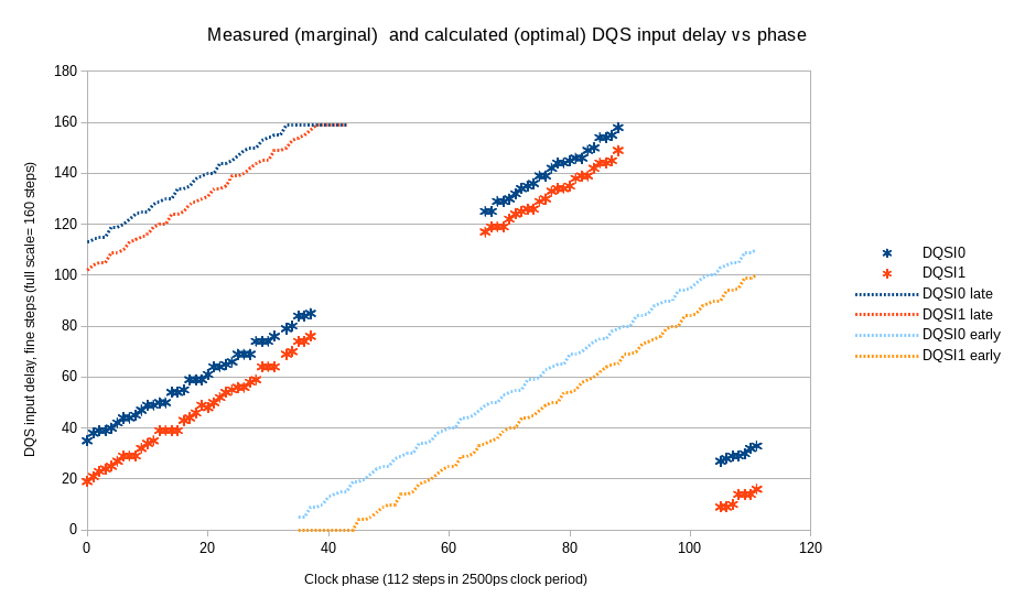
Fig.7 Measured (marginal) and calculated (optimal) DQS input delays vs. clock phase
Data is crossing clock domains boundary at a single clock rate (2 bits at a time for each data line), so using fixed pattern of alternating 0-1-0-1… can not be used – regardless of the phase shift it will be the same “01” pair. For this reason we use actual read data command, not a special read pattern mode. Random data that is present in the memory array after power up can be used, but the program is writing a 0-0-1-1-0-0- 11… pattern for each data bit. This pattern will provide different di-bit value in each DQ line, even if the write DQ to DQS timing is not yet determined, so the actual data can be any of X-0-X-1-X- 0… where X can quasi-randomly be any of 0 or 1. The pattern is recorded once, then the data is read with different DQS input delays (DQ input delays are set according to step 4 results), comparing only the middle portion with the beginning/end discarded as before. The marginal DQS delay is detected as the value when the read data changes from the original value.
Figure 7 shows results of such measurements as well as the calculated optimal input delays for DQS lines. This calculation uses both Step 5 (DQS vs. phase) and Step 4 (DQ vs. DQS) measuremts and accounts for the fine delay non-uniformity.
Step 6: DQ to DQS output delays measurements
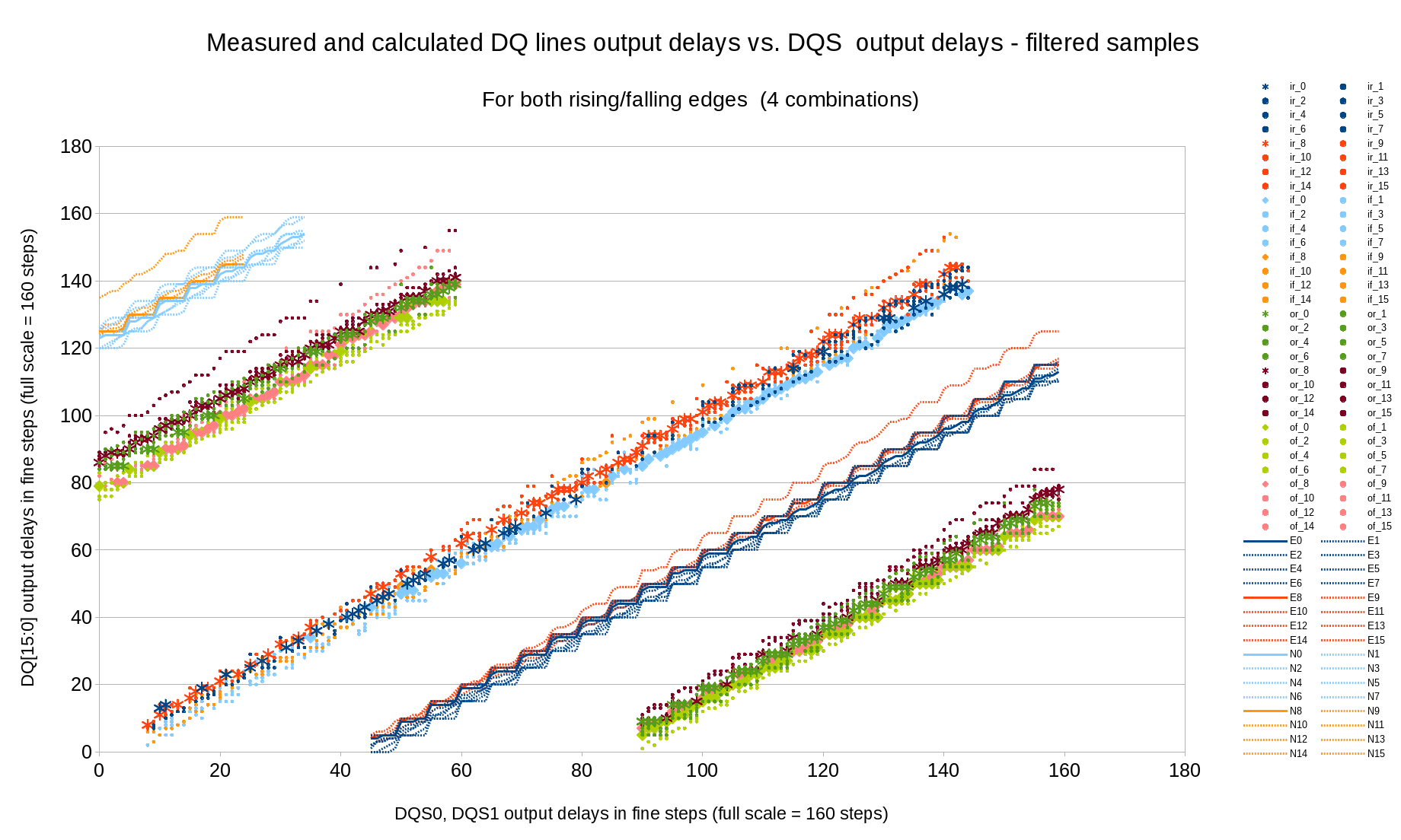
Fig.8 Measured (marginal) and calculated (optimal) DQ input delays vs. DQS output delays
This measurement is performed similarly to step 4 when DQ to DQS input delays relation was probed with a fixed pattern readout mode. Now we already have known settings for the memory read operation and can rely on it to adjust write mode (output) delays. Alternating 0-1-0-1 sequence in every line similar to the pattern mode is recorded with various DQS output delay values, for each DQS delay appropriate phase and address/command delay values are used. Input delays (for DQS and DQ) are set for each phase using data from the previous steps and the data written with different DQ output delay is read back, then processed in the same way as in Step 4.
Figure 8 presents the relation between DQ and DQS output delays, and the result of combining Step 6 measurements with Step 3 (write levelling) – optimal DQ and DQS output delay values for different clock phase can be seen on Figure 9 that shows all the delays. Allowing some deviation from the DQS to clock alignment (this requirement is more relaxed than DQ-to-DQS delays) results into 2 alternative solutions for the same phase shift near phase=95, use of the higher memory clock rates will result in more of such multi-solution areas even without deviation from the optimal values.
Step 7: Measuring individual output delays for all address and bank lines
Having almost calibrated read and write memory operations it is now possible to set up output delays for each of the remaining address and bank lines (so far only A[7] was measured, other lines were just assumed to be the same). This measurement is done with writing some “good” pattern to a specific bank/row/column page (column address uses the low bits of the row address), and a “bad” data to all pages different by 1 of the address or bank bits. For this test the refresh sequence (it is loaded by the software, it is not hard-wired in the HDL code) was modified to provide specified data on the bank/address lines that is “don’t care” for this operation. These values are set to be inverted values to the “good” address, and the refresh command was manually requested before the read operation, making sure that the command will cause all the address/bank bits to be inverted.
All the phase values are scanned, for each phase the command and address delays are set to the optimal values as defined so far, and only one line at a time delay was modified to find the marginal value that causes the readout of the wrong data block.
This measurement is performed twice – fist with “good” address of all zeros, then – with all ones and results averaged for low → high and high → low address line transitions.
Step 8: Selecting valid parameter combinations for readout and write modes
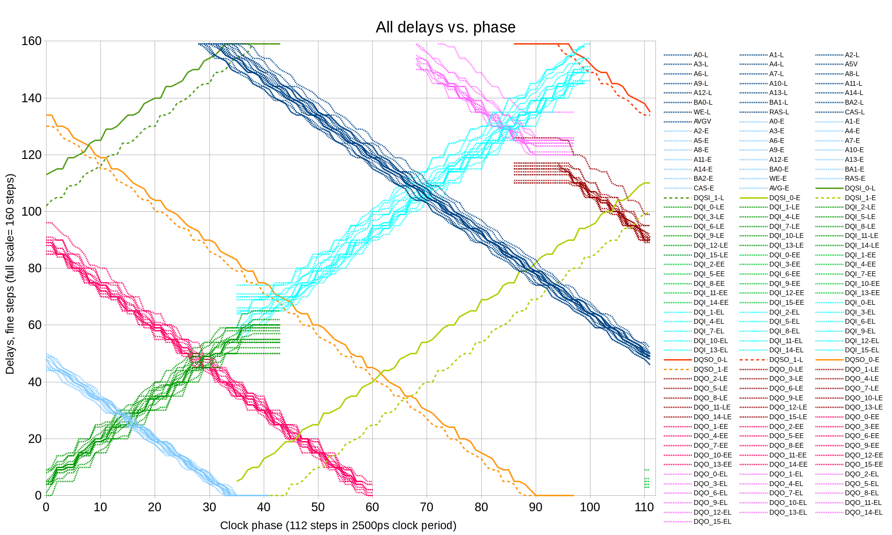
Fig.9 All delays vs. clock phase
Figure 9 combines all the data acquired so far as a function of the clock phase shift. Most of the delays do not change when the new bitstream is generated after the modification of the HDL code – the involved delays are defined by the fixed I/O circuitry and PCB/package routing. Only two of the signals involve FPGA fabric routes – DQS input signals that include BUFIO clock buffers, these buffers can be selected differently and routed differently by the tools. These signals also show the largest difference one the graph (two pairs of the green lines – solid and dashed).
There are additional requirements that are not shown on the Figure 9. DQ signals from the memory should arrive to the deserializer ¼ clock period earlier than the leading edge of the first DQS pulse, not 1 ¼ or not ¾ later – the measurements so far where made to the nearest clock period. Memory device generates exactly the required number of DQS transitions, so if the data arrives 1 clock too early, then the first two words will be lost, if it arrives 1 clock too late – the last two words will be lost.
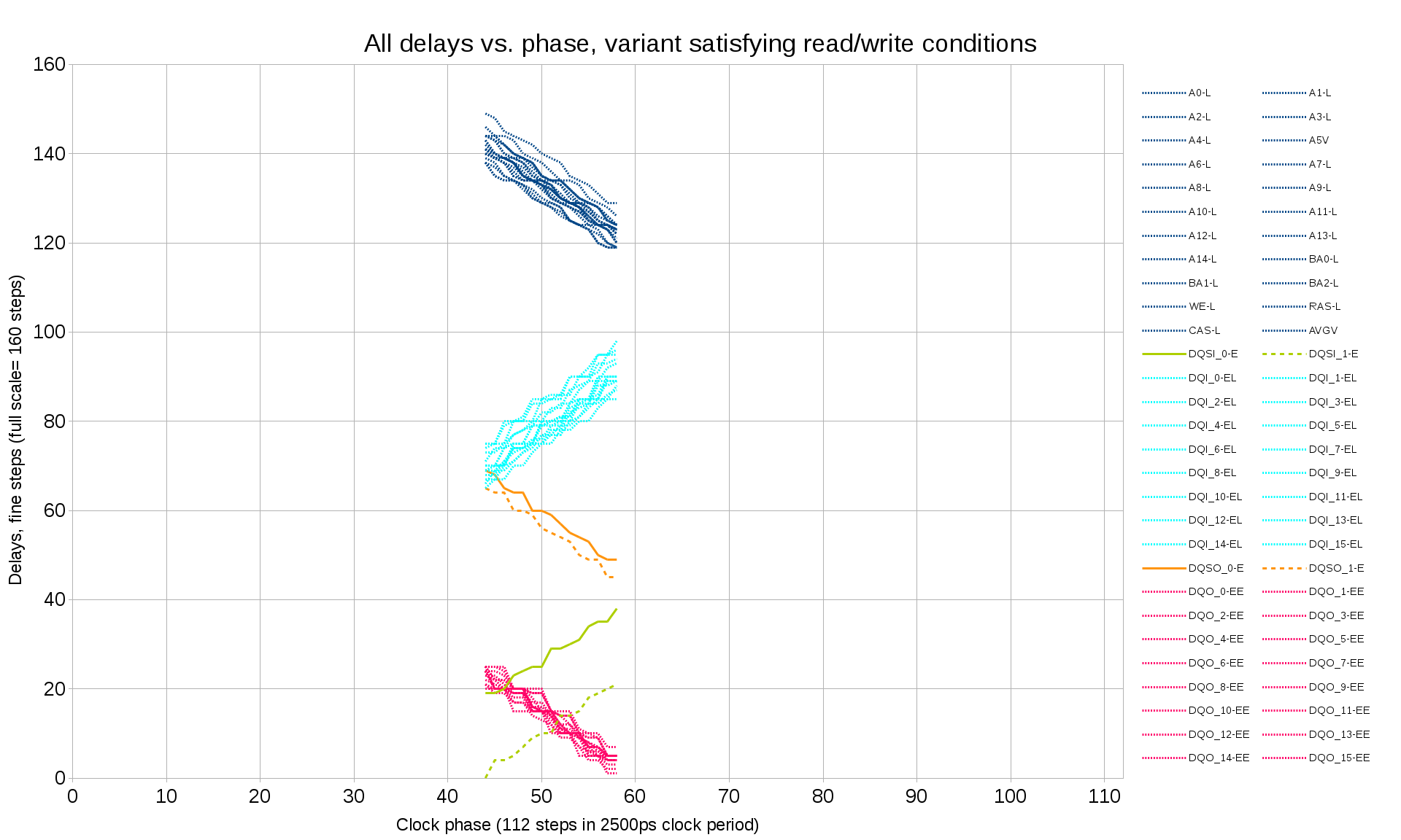
Fig.10 All delays vs. clock phase, filtered to satisfy period-correct write/read conditions
For this final step the alternative variants of the setting that differ by the full clock periods are selected and tested. First the block with incremented (each word is the previous one plus 1) data is recorded and then the smaller block completely inside the recorded one and not using the first/last bursts is read back. The write mode is not yet set up, so the first/last recorded burst can not be trusted, but the middle ones should be recorded incrementally, so any differences from this pattern have to be caused by the incorrect readout settings.
After removing invalid parameter combinations defining the readout mode we can trust that the full block readout has all the words valid. Then we can do the same for the write mode and check which of the variants (if any) provide correct memory write operation. In the test case (one particular hardware sample and one clock frequency there was exactly one variant (as shown on the Figure 10) and the final settings can use the center of the range. With higher clock frequency several solutions may be possible – then other factors can be considered, such as trying to minimize the delays of the most timing-critical signals (DQ, DQS) to reduce dependence on the possible delay vs. temperature variations (not measured yet).
Model and parameters of the input/output delay elements
Processing of the measurement results in steps 4 and 6 involved using a delay model defined by a set of parameters and then finding the values of these parameters to best fit the measurement results.
Each data byte lane is independent from the other, so for each of the 4 groups (two for output and two for input) there are nine signals – one DQS and 8 DQ signals. Each delay consists of a 32-tap delay line with the datasheet delay of 78 ps per tap and a 5-tap delay with nominal 10 ps step. Our model represents each 32-tap delay as linear with tDQ[7:0] delays corresponding to a tap 0 and tSDQ[7:0], tSDQS – individual scale (measured in picoseconds per step). Fine delay steps turned out to be very non-uniform (in some cases even non-monotonic) so each of the 4 delay values (for 5-tap delay) is assigned an individual parameter – 4 for DQS (tFSDQS) and 32 for DQ (tFSDQ).
Procedure of measuring all 4 combinations of leading/trailing edges of the strobe and data makes it possible to calculate duty cycle for each of the 9 signals – tDQSHL (difference between time high and time low for the DQS signal) and eight tDQHL[7:0] for the similar differences for each of the data lines. Additional parameter was used to model the uncertainty of the measurement results (number of ones or zeros of the 32 samples) as a function of the delay difference from the center (corresponding to 50% of the zeros and ones). This parameter (anaScale in the program code) is measured in picoseconds and means how much the delay should be changed to switch form all 0 to all 1 (using simple piecewise linear approximation).
Parameter fitting is implemented using Levenberg-Marquardt algorithm, initial scale values use dataseeet data, initial delays are estimated using histograms of the acquired data (to separate data acquired with different integer number of clock cycles shift), other parameters are initialized to zeros. Below is a sample of the program output – algorithm converges rather quickly, getting to the remaining root mean square error (difference between the measured and modeled data) of about 10ps:
Before LMA (DQ lane 0): average(fx)= 40.929028ps, rms(fx)=68.575944ps

0: LMA_step SUCCESS average(fx)= -0.336785ps, rms(fx)=19.860737ps

1: LMA_step SUCCESS average(fx)= -0.588623ps, rms(fx)=11.372493ps

2: LMA_step SUCCESS average(fx)= -0.188890ps, rms(fx)=10.078727ps

3: LMA_step SUCCESS average(fx)= -0.050376ps, rms(fx)=9.963139ps

4: LMA_step SUCCESS average(fx)= -0.013543ps, rms(fx)=9.953569ps

5: LMA_step SUCCESS average(fx)= -0.003575ps, rms(fx)=9.952006ps

6: LMA_step SUCCESS average(fx)= -0.000679ps, rms(fx)=9.951826ps
Tables 1 and 2 summarize parameters of delay models for all input and data/strobe output signals. Of course these parameters do not describe the pure delay elements of the FPGA device, but a combination of these elements, I/O ports and PCB traces, delays in the DDR3 memory device. The BUFIO clock buffers and routing delays also contribute to the delays of the DQS input paths.
| parameter | number of values | average | min | max | max-min | units |
|---|---|---|---|---|---|---|
| tDQSHL | 2 | 4.67 | -35.56 | 44.9 | 80.46 | ps |
| tDQHL | 16 | -74.12 | -128.03 | -4.96 | 123.07 | ps |
| tDQ | 16 | 159.87 | 113.93 | 213.44 | 99.51 | ps |
| tSDQS | 2 | 77.98 | 75.36 | 80.59 | 5.23 | ps/step |
| tSDQ | 16 | 75.18 | 73 | 77 | 4 | ps/step |
| tFSDQS | 8 | 5.78 | -1.01 | 9.88 | 10.89 | ps/step |
| tFSDQ | 64 | 6.73 | -1.68 | 14.25 | 15.93 | ps/step |
| anaScale | 2 | 17.6 | 17.15 | 18.05 | 0.9 | ps |
| parameter | number of values | average | min | max | max-min | units |
|---|---|---|---|---|---|---|
| tDQSHL | 2 | -114.44 | -138.77 | -90.1 | 48.66 | ps |
| tDQHL | 16 | -23.62 | -96.51 | 44.82 | 141.33 | ps |
| tDQ | 16 | 1236.69 | 1183 | 1281.92 | 98.92 | ps |
| tSDQS | 2 | 74.89 | 74.86 | 74.92 | 0.06 | ps/step |
| tSDQ | 16 | 75.42 | 69.26 | 77.22 | 7.96 | ps/step |
| tFSDQS | 8 | 6.16 | 2.1 | 11.32 | 9.22 | ps/step |
| tFSDQ | 64 | 6.94 | 0.19 | 19.81 | 19.63 | ps/step |
| anaScale | 2 | 8.18 | 5.38 | 10.97 | 5.59 | ps |
Features I would like to see improved in the future Xilinx devices
“Finedelay” 5-delay delay stage in IDELAY2 and ODELAY2 elements
I noticed the existence of these 5-tap delay elements in the utilization report of Xilinx Vivado tools – they do not seem to be documented in the Libraries Guide. I assume that the manufacturer was not very happy with their performance (the average measured value of the delay per tap turned out to be less than 7 ps so even the last tap output does not provide delay of the half of the 32-tap step, and non-uniformity of the delays makes it difficult to use in the simple hardware-based delay adjustment modules. But I like this option – it almost gives one extra bit of delay and as we are using software for delay calibration it is not a problem to have even a non-monotonic delay stage. So I would like to see this feature improved – added more taps to completely cover the full step of the coarse delay stage in the future devices, and have this nice feature documented, not hidden from the users.
Use of the internal voltage reference and the duty cycle correction
Internal reference voltage option was used in the tested circuitry because of the limited number of pins to implement a single-bank 16-bit wide memory interface, and the Xilinx datasheet limits memory clock to just 400 MHz for such configuration. Measurements show that there is a bias of -74.12ps on the duty cycle that may be caused by variation of the internal reference voltage, but the spread of the delays (123 ps) is still larger. Of course it is difficult to judge without having statistics on multiple units, but I suppose that the handicap of using internal reference is not that significant. And even 123ps is not that big as tDQHL was measured as a difference of duration high minus duration low, so if one transition edge is fixed, the other will have an error of just half of this value – less than a coarse (32-tap) delay when calibrated at 200 MHz (fine delay is possible to calibrate with 300MHz).
It would be nice to have at least a couple of bits in the delay primitives dedicated to the duty cycle correction of the delay elements that can be implemented as selective AND or OR the delay tap output with the previous one.
Hello,
Great work! I am a little un-clear about your setup though. You are running python on the hardware => the hardware is already running Linux => the DDR3 interface is already working. May I ask if my understanding is correct? You mention that the calibration routine has to be run only once (the first time and takes 10mins), but even to run once doesn’t the hardware need to be up and running?
Thanks,
Camera has 3 identical memory chips (http://wiki.elphel.com/images/5/53/10393_bd.png, http://wiki.elphel.com/images/f/fd/10393.pdf) – 2 make x32 system memory, the third one – FPGA dedicated memory. System memory is trained by the boot loader at start up time – before Linux and even UBoot is loaded. Xilinx software uses FSBL, we use https://github.com/Elphel/ezynq for that.
The elaborate memory calibration is only needed for the FPGA part.
Running at 800 Mb/s (@400 MHz clock) even with the internal voltage reference we can use the same presets – results of a single camera calibration. We will use the full capabilities of the software to increase memory clock to the limit Zynq will be able to handle.