DDR3 Memory Interface on Xilinx Zynq SOC – Free Software Compatible
External memory controller is an important part of many FPGA-centered designs, it is true for Elphel cameras too. When I was working on the board design for NC393 I tried to verify inteface pinout using the code output from the MIG (Memory Interface Generator) module. I was planning to use MIG code as a reference design and customize it for application in the camera, adding more functionality to our previous designs. Memory interface is a rather intimate part of the design where FPGA approach can shine it all its glory – advance knowledge of the types of needed memory transactions (in contrast with the general CPU system memory) helps to increase performance by planning bank and address sequences, crafting memory mapping to utilize close to 100% of the bus bandwidth.
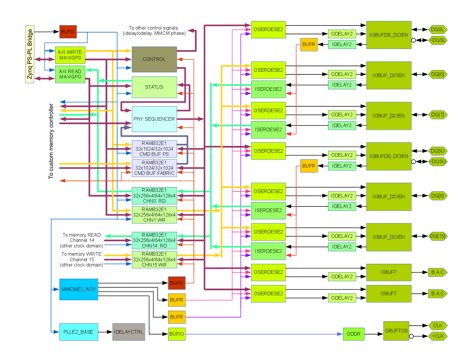
Fig. 1. DDR3 memory controller block diagram, source code at https://git.elphel.com/Elphel/eddr3
Contents
- 1 Why new DDR3 controller when Xilinx provides MIG?
- 2 Does that mean that Zynq SOC is completely useless for Elphel projects?
- 3 DDR3 memory interface requirements
- 4 DDR3 Interface Implementation
- 5 EDDR3 Performance Evaluation
- 5.1 DQ and DQS input delay selection by reading fixed pattern from memory
- 5.2 Scanning DQS input delay with fixed DQ input delay using randomly generated data
- 5.3 Aligning individual DQ input delay values
- 5.4 Scanning over DQS input delay with DQ input delays aligned
- 5.5 Evaluation of memory WRITE operations
- 5.6 Scanning over DQS output delay with the individual DQ output delays programmed to the same value
- 5.7 Aligning individual DQ output delay values
- 5.8 Scanning over DQS output delays with the individual data bits aligned
- 6 Software Tools Used
- 7 Conclusions
Why new DDR3 controller when Xilinx provides MIG?
That was my original plan, but MIG code used 6 undocumented modules (PHASER_*,PHY_CONTROL) and four more (ISERDESE2,OSERDESE2,IN_FIFO and OUT_FIFO) that are only partially documented and the source code of the simulation modules is not available to Xilinx users.
This means that MIG as it is currently provided by Xilinx does not satisfy our requirements. It would prevent our customers from simulating Elphel code with Free Software tools, and it also would not allow us to develop efficient code ourselves. Developing HDL code, troubleshooting complex cases through simulation is a rather challenging task already, guessing what is going on inside the “black boxes” without the possibility to at least add some debug output there – it would be a nightmare. Why does the signal differs from what I expected – is it one of my stupid assumptions that are wrong in this case? Did I understand documentation incorrectly? Or is there just a bug in that secret no-source-code module? I browsed the Internet support forums and found that yes, there are in fact cases where users have questions about the simulation of the encrypted modules but I could not find clear answers to them. And it is understandable – it is usually difficult to help with the design made by somebody else, especially when that encrypted black box is connected to the customer code that differs from what black box developers had in mind themselves.
Does that mean that Zynq SOC is completely useless for Elphel projects?
Efficient connection to the dedicated (not shared with the CPU) high performance memory is a strict requirement for Elphel products and Xilinx FPGA were always very instrumental in achieving this goal. Through more than a decade of developing cameras based on Xilinx programmable logic our cameras used SDR, then DDR and later DDR2 memory devices. After discovering that while advancing silicon technology Xilinx made a step back in the quality of the documentation and simulation support I analyzed the set of still usable modules and features of this new device to see if they alone are sufficient for our requirements.
The most important are serializer, deserializer and programmable delay elements (in both input and output directions) on each I/O pin connected to the memory device, and Xilinx Zynq does provide them.
The OSERDES2 and ISERDESE2 (serializer and deserializer modules in Xilinx Zynq) can not be simulated with Free Software tools directly as they depend on encrypted code, but their functionality (without undocumented MEMORY_DDR3 mode) matches that of Xilinx Virtex 6 devices. So with the simple wrapper modules that switch between the *SERDESE2 for synthesis with Xilinx tools and *SERDESE1 for simulation with Icarus Verilog simulator that problem was solved.
Input/output delay modules have their HDL source available and did not cause any simulation problems, so the minimal requirements were met and the project goals seemed possible to achieve.
DDR3 memory interface requirements
Looking at the Xilinx MIG implementation I compared it with our requirements and I’ve got an impression it tried to be the single universal solution for every possible application. I do not agree with such approach that contradicts the very essence of the FPGA solutions – possibility to generate “hardware” that best suits the custom application. Some universal high-level hard modules enhance bare FPGA fabric – such elements as RAM blocks, DSP, CPU – these units being specialized lost some of their flexibility (compared to than arbitrary HDL code) but became adopted by the industry and users as they offer high performance while maintaining reasonable universality – same modules can be reused in numerous applications developed by users. The lack of possibility to modify hard modules beyond provided configurable options comes as understandable price for performance – these limitations are imposed by the nature of the technology, not by the bad (or good – trying to keep inexperienced developers away from the dangers of the unrestricted FPGA design) will of the vendors.
Below is the table that compares our requirements (and acceptable limitations) of the DDR3 memory interface in comparison with Xilinx MIG solution.
Feature comparison table
| Feature | MIG | eddr3 | notes |
|---|---|---|---|
| Usable banks | HP,HR | HP only | HR I/O do not support output delays and limit DCI |
| Data width | any | 16 bits | Data width can be manually modified |
| Multi-rank support | yes | no | Not required for most applications |
| FBG484 single bank | no | yes | MIG does not allow 256Mx16 memory use one bank in FBG484 package |
| Access type | any | block oriented | Overlapping between accesses may may be disregarded |
| R/W activity | on-the-fly | pre-calculated | Bank mapping, access sequences pre-calculated in advance |
| Initialization, leveling | hardware | software | Infrequent procedures implemented in software |
| Undocumented features | yes | no | Difficult to debug the code |
| Encrypted modules | yes | no | Impossible to simulate with Free Software tools, difficult to debug |
| License | proprietary | GNU GPLv3.0+ | Proprietary license complicates distribution of derivative code |
Usable I/O banks
Accepting HR or “high (voltage) range” banks for memory interfacing lead MIG to sacrifice the ODELAYE2 blocks that are available in HP (“high performance”) banks only. And we did not have this limitation, as the DDR3 chip was already connected to HP bank. I believe it is true for other designs too – it makes sense do follow the bank specialization and use memory with HP banks and reserve HR for other application (like I/O) where the higher voltage range is actually needed.
Block accesses only
Another consideration is that having abundance of 32Kb block memory resources in the FPGA and parallel processing nature of the programmable logic, the small memory accesses are not likely, many applications do not need to bother with reduced burst sizes, data byte masking or even back-to-back reads and writes. In our applications we use 1/4 of the BRAM size transfers in most cases (1/4 comes from having a 4-page buffer at each channel to implement simple 2-level prioritizing between multiple channels. Block access does not have to be limited to memory pages – it can be any large predefined sequences of data transfer.
Hardware vs software implementation of infrequent actions
MIG feature that I think leads to unneeded complication – everything is done in “hardware”, even write leveling and temperature compensation from the on-chip temperature sensor. I was once impressed by the circuit diagram of Apple ][ computer, and learned a lesson that you do not need to waste special hardware resources on what easily can be done in software without significant sacrifice of performance. Especially in the case of a SOC like Zynq where a high-performance dual-core processor is available. Algorithms that need to run once at start-up and very infrequently during operation (temperature correction) can easily be implemented in software. The memory controller implemented in PL is initialized when the system is fully loaded, so initialization and training can be performed when the full software is available, it is not as system memory that has to be operational from the early boot stage.
Computation of the access sequences in advance
When dealing with the multi-channel block access (blocks do not need to be the same size and shape) in the camera, it is acceptable to have an extra latency comparable to the block read/write time, that allowed to simplify the design (and make it more flexible at the same time) by splitting generation and execution of the block access sequences in two separate processes. The physical interface sequencer reads the commands, memory addresses and control signals (as well as channel buffer read/write enable from the block memory, the sequence data is prepared in advance from 2 sources: custom PL circuitry that calculates the next block access sequence and loaded directly by the software over AXI channel (refresh, calibrate ZQ, write leveling and other delay measurement/adjustment sequences)
No multi-rank
Another simplification – I did not plan to use multi-rank systems, supplementing FPGA with just one (or several, but just to increase data width/bandwidth, not the depth/capacity) high performance memory chip is a most common configuration. Internal data paths of the programmable logic have so much higher bandwidth than the connection to an external memory, that when several memory chips are used they are usually connected to achieve the highest possible bandwidth. Of course, these considerations are usually, but not always valid. And the FPGA are very good for creating custom solutions for particular cases, not just “one size fits all”.
DDR3 Interface Implementation
Fig. 1 shows simplified block diagram of the eddr3 project module. It uses just one block (HP34) for interfacing 512M x 16 DDR3 memory with pinout following Xilinx recommendations for MIG. There are two identical byte lanes each having 8 bidirectional data signals running in DDR mode (DQ[0]..DQ[7] and DQ[8]..DQ[15] – only two bits per lane are shown on the diagram), one bidirectional differential DQS. There is also data mask (DM) signal in each byte lane – it is similar to DQ without input signal, and while it is supported in the physical level of the interface, it is not currently used on a higher level of the controller. There is also a differential driver for the memory clock input (CLK,~CLK) and address/command signals that are output only and run in SDR mode at the clock rate.
I/O ports
Data bit I/O buffers (IOBUF_DCIEN modules) are directly connected to the I/O pads produce read data outputs feeding IDELAYE2 modules, have data inputs for the write data coming form ODELAYE2 modules, output tristate control and DCI enable inputs. There is only one output delay unit per bit, so tristate control has to come directly from the OSERDESE2 module, but that is OK as the it is still possible to meet the memory requirements when controlling tristate at clock half-period granularity, even when switching between read and write commands. But in the block-oriented memory access in the camera it is even easier as there are no back-to-back read to write accesses. DCIEN control is even less timing critical – basically it is just a power reduction feature so turning it off later and turning on earlier than needed is acceptable. This signal is controlled with the clock period granularity, same as address/command signals.
Delay elements
ODELAYE2 and IDEALYE2 provide 5-bit (31-tap) programmable delays with 78 ps/tap resolution for 200MHz calibration and 52 ps tap for 300MHz one. The device I have on the prototype board has speed grade 1 so I was limited to 200MHz only (300MHz option is only available for the speed grade 2 or higher devices). From the tools output I noticed that these primitives have *_FINEDELAY option and while these primitives are not documented in Libraries Guide they are in fact available in unisims library so I decided to take a risk and try them, tools happily accepted such code. According to the code FINEDELAY option provides additional stage with five levels of delay with uncalibrated 10 ps step and just static multiplexer control though the 3 inputs. It will be great if Xilinx will add 3 more taps to use all 3 bits of fine delay value the delay range of this stage will cover the full distance between the outputs of the main (31-tap) delay. It is OK if the combined 8-bit (5+3) delay will not provide monotonic results, that can be handled by the software in most cases. With current hardware the maximal delay of the fine stage only reaches the middle between the main stage taps (4*10 ps ~= 78 ps/2), so it adds just one extra bit of resolution, but even that one bit is very helpful in interfacing DDR3 memory. The actual hardware measurements confirmed that the fine delay stage functions as expected and that there are only 5 steps there. Fine delay stage does not have memory registers to support load/set operations as the main stage, so I added it with additional HDL code. The fine delay mode applies to all IDEALYE2 and ODELAYE2 block shown on the diagram, each 8-bit delay value is individually loaded by software through MAXIGP0 channel, additional write sets all the delays simultaneously.
Source-synchronous clocks
Received DQS signal in each byte lane goes through input delay and then drives BUFR primitive that in turn provides input clock to all data bit ISERDESE2 modules in the same byte lane. I tried to use BUFIO for that purpose, but the tools did not agree with me.
Serializers and deserializers, clocks
The two other clocks driving ISERDESE2 and OSERDESE2 (they have to be the same for input and output paths) are generated by the MMCME2_ADV module. One of them is the full memory clock rate, the other has half frequency. The same MMCME2_ADV module generates another half frequency clock that through the global buffer BUFG drives the rest the controller, registers are inserted in the data paths crossing clock domains to compensate for possible phase variations between BUFG and BUFR. Additional output drives memory clock input pair, MMCME2_ADV dynamically phase shifts all the other outputs but this one, effectively adding one extra degree of freedom for meeting write leveling requirements (zero phase shift between clock and DQS outputs). This clock control is implemented in phy_top.v module.
I/O delay calibration
PLLE2_BASE is used to generate 200MHz used for calibration of the input/output delays by the instance of IDELAYCTRL primitive.
PHY control sequencer
The control signals: memory addresses/bank addresses, commands, read/write enable signals to channel data buffers are generated by the sequencer module running at half of the memory clock, so the width of data read/write to the data buffers is 64 bits for 16 bit DDR3 memory bus. Sequencer data is encoded as 32-bit words and is provided by the multiplexed output from the read port of one of the two parallel memory blocks. One of these block is written by software, the other one is calculated in the fabric. Primary application is to read/write block data to/from multiple concurrent channels (for NC393 camera we plan to use 16 such channels), and with each channel buffer accommodating 4 blocks it is acceptable to have significant latency in the data channels. And I decided to calculate the control data separately from accessing the memory, not to do that on-the-fly. That simplifies the logic, adds flexibility to optimize sequences and with software programmable memory it simplifies evaluation of different accesses without reconfiguring the FPGA fabric.
In the current implementation only one non-NOP command can be issued in the sequencer 2-clock time slot, but which clock to use – first or second is controlled by a program word bit individually for each slot. Another bit adds a NOP cycle after the current command, this is used for bulk of the read/write commands for consecutive burst of 8 accesses. When the sequencer command is NOP the address fields are re-used to specify duration of the pause and the end-of-sequence flag.
CPU interface, AXI port
Initial implementation goal was just to test the memory interface, it has only two (instead of 16) memory access channels – program read and program write data, and there is only one of the two sequencer memory banks (also programmed by the software), the only asynchronously running channel is memory refresh channel. All the communications are performed over AXI PS Master GP0 channel with memory mapped addresses for the controller configuration, delays and MMCM phase set up, access to the sequencer and data memory. All the internal clocks are derived from a single (currently 50MHz) FCLKCLK[0] clock coming from the PS7 module (PS-PL bridge), EMIO pins are used for debugging only.
EDDR3 Performance Evaluation
Current implementation uses internal Vref and the Zynq datasheet specifies the maximal clock rate 400MHz (800 Mb/s) rate so I started evaluation at the same frequency. But the memory chip connected to Zynq is Micron MT41K256M16HA-107:E (same as the other two used for the system memory) capable of running at 933MHz, so the plan was to increase the operational frequency later, so 400 MHz clock (1600MB/s for x16 memory) is sufficient just to start porting our earlier camera functionality to the Zynq-based NC393. Initial settings for all output and I/O ports SLEW is “SLOW” so the inter-symbol interference should reveal itself at lower frequencies during evaluation. Power supply voltage for the HP34 port and memory device is set to 1.5V, hardware allows to reduce it to 1.35V so later we plan to evaluate 1.35V performance also.
Performance measurements are implemented as a Python script (it does not look like Pythonian, most of the text was just edited from the Verilog text fixture used for simulation) running on the target system, the results were imported into Libreoffice Calc spreadsheet program to create eye diagram plots. Python script directly accesses memory-mapped AXI PS Master GP0 port to read/write data, no custom kernel space drivers were needed for this project. Both simulation test fixture and the Python script programmed delay values, controller modes and created sequence data for memory initialization, refresh, write leveling, fixed pattern reading, block write and block read operations. For eye pattern generation one of the delay values was scanned over the available range, randomly generated 512 byte block of data was written and then read back. Then the read data was compared to the one written, each of the 4096 bits in a block was assigned a group depending on the previous, current and next bit written to the same DQ signal. These groups are shown on the next plots, marked in the legend as binary strings, “001” means that previous written bit was “0”, current one is also “0” and the next one will be “1”. Then the read data was averaged in each block per each of 8 groups, first for each DQ individually and averaged between all of the 16 DQ signals. The delays scanned over 32 values of the main delays and 5 values of fine delays for each, the relative weight of fine delays was calculated from the measured data and used in the final plots.
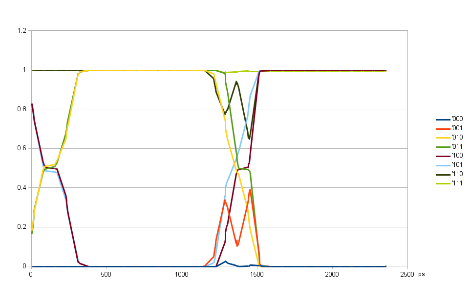
Fig. 2. DQ input delay common for all bits, DQS input delay variable
DQ and DQS input delay selection by reading fixed pattern from memory
First I selected initial values for DQ and DQS input delays reading fixed pattern data form the memory – that mode eliminates dependence on write operation errors, but does not allow testing over the random data, each bit toggles simultaneously between zero and one. This is a special mode of DDR3 memory devices activated by control bits in the MR3 mode register, reading this pattern does not require activation or any other commands before issuing READ command.
Scanning DQS input delay with fixed DQ input delay using randomly generated data
DQ delays can scan over the full period, but DQS input delay has certain timing dependence on the pair of output clock. Fig. 2. illustrates this – the first transition centered at ~150 ps is caused by the relative input delays of DQ and DQS. Data strobe latches mostly previous bit at delays around 0 and correctly latches the current bit for delays form 400 to 1150 ps, then switches to the next bit. And at around the same delay of 1300 ps the iclk to oclk timing in ISERDESE2 is not satisfied causing errors not related to DQ to DQS timing. The wide transition at 150 ps is caused by a mismatch between individual bit delays, when those individual bits are aligned (Fig. 4) the transition is narrower.
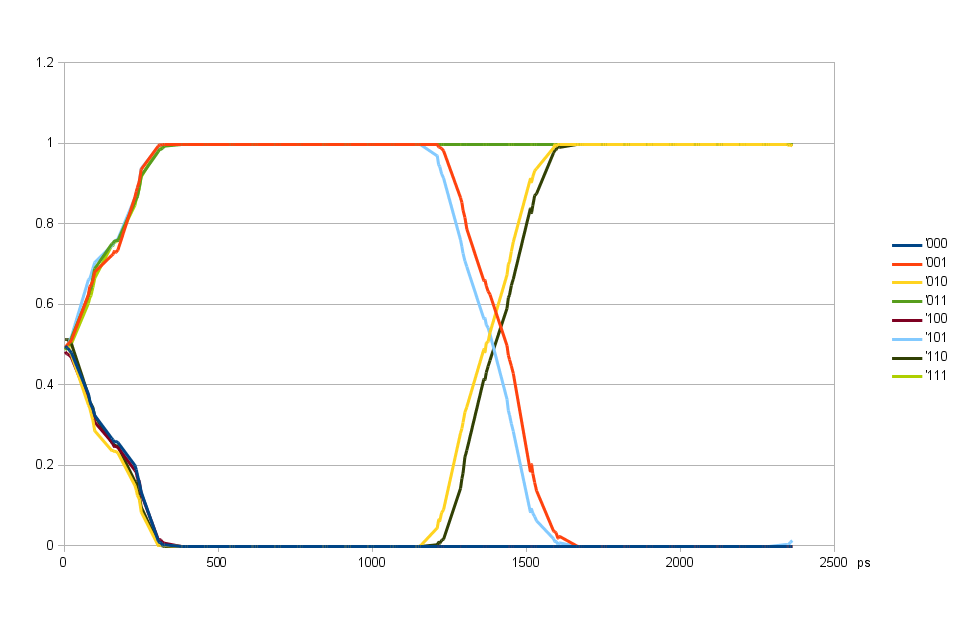
Fig. 3. Alignment of individual DQ input delays using 90-degree shifted DQS delay
Aligning individual DQ input delay values
For aligning individual DQ input delays (Fig. 3) I programmed DQS 90 degrees offset from the eye center of Fig. 2, and find the delay value for each bit that provides the closest to 50% value.
Scanning takes over both main (32 steps) and fine (5 steps) delays, there are no special requirements on the relative weights of the two, no need for the combined 8-bit delay to be monotonic. This eye patter doe not have an abnormality similar to the one for DQS input delay, the result plot only depends on DQ to DQS delay, there are no additional timing requirements. The transition ranges are wide, plot averages results from all individual bits, alignment process uses individual bits data.
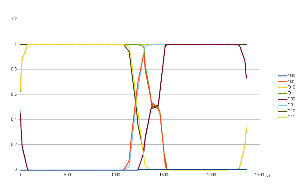
Fig.4. DQ input delays aligned, DQS input delay variable
Scanning over DQS input delay with DQ input delays aligned
After finishing individual data bits (DQ) input delays alignment I measured the eye pattern for DQS input delay again. This time the eye opened more as one of the sources of errors was greatly diminished. Valid data is now from 100 ps to 1050 ps and DQS delay can be set to 575 ps in the center between the two transitions. At the same time there is more than 90 degrees phase shift of the DQS from the value when iclk to oclk delay causes errors.
Fig.4. also shows that (at ~1150 ps) there is very little difference between 010 and 110 patterns, same for 001 and 101 pair. That means that inter-symbol interference is low and the bandwidth of the read data transfer is high so the data rate can likely be significantly increased.
Evaluation of memory WRITE operations
When data is written to memory DDR3 device is expecting certain (90 degree shift) timing relation between DQS output and DQ signals. And similar to the read operation there are additional restrictions on the DQS timing itself. The read DQS timing restrictions were imposed by the ISERDESE2 modules, in the case of write the DQS timing requirements come form the memory device – DQS should be nominally aligned to the clock on the input pads of the memory device. And there is a special mode supported by DDR3 memory devices to facilitate this process – “write leveling” mode – the only mode when memory uses DQS as input (as in WRITE modes) and drives DQ as outputs (as in READ mode), with least significant bit in each byte lane signals the level of clock signal at DQS rising edge. By varying the DQS phase and reading data it is possible to find the proper delay of the DQS output, additionally the relative memory clock phase is controlled by the programmable delay in the MMCME2_ADV module.
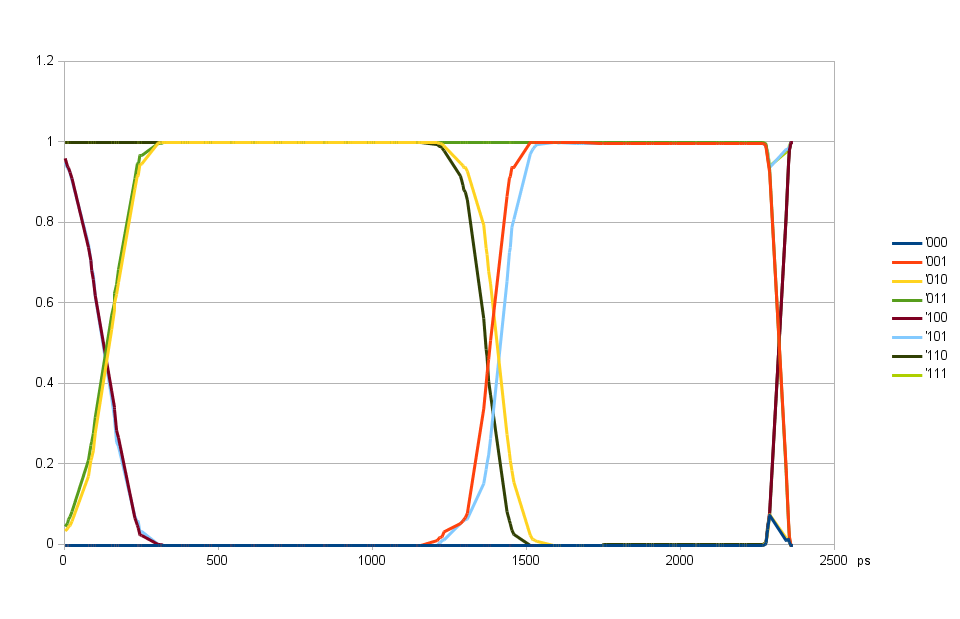
Fig. 5. DQ output delay common for all bits, DQS output delay variable
Scanning over DQS output delay with the individual DQ output delays programmed to the same value
With the DQ and DQS input delays determined earlier and set to the middle of the respective ranges it is possible to use random data writing to memory for evaluation of the eye patterns for WRITE mode. Fig. 5. shows the result of scanning of the DQS output delay over the full available range while all the DQ output delays were set to the same value of 1400 ps. The optimal DQS output delay value determined by write leveling was 775 ps. The plot shows the only abnormality at ~2300 ps caused by a gross violation of the write leveling timing, but this delay is far from the area of interest and results show that it is safe to program the DQS delay off by 90 degrees from the final value for the purpose of aligning DQ delays to each other.
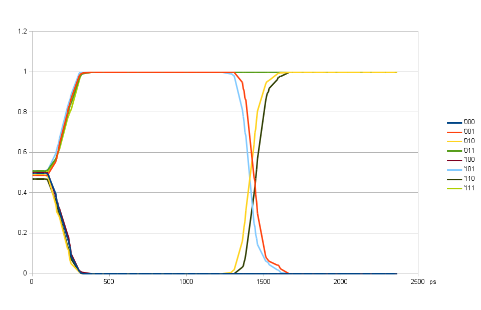
Fig. 6. Alignment of individual DQ output delays using 90-degree shifted DQS output delay
Aligning individual DQ output delay values
The output delay of the individual DQ signals is adjusted similarly to how it was done for the input delays. The DQS output delay was programmed with 90 degree offset to the required value (1400 ps instead of 775 ps) and each data bit output delay was set to the value that results in as close to 50% as possible. This condition is achieved around 1450 ps as shown on the Fig. 6.
50% level at low delays (<150 ps) on the plot comes from the fact that the bit “history” is followed to only 1 before the current, and the range of the Fig. 6 is not centered around the current bit, it covers the range of two bits before current, 1 bit before current and the current bit. And as two bits before current are not considered, the result is the average of approximately equal probabilities of one and zero.
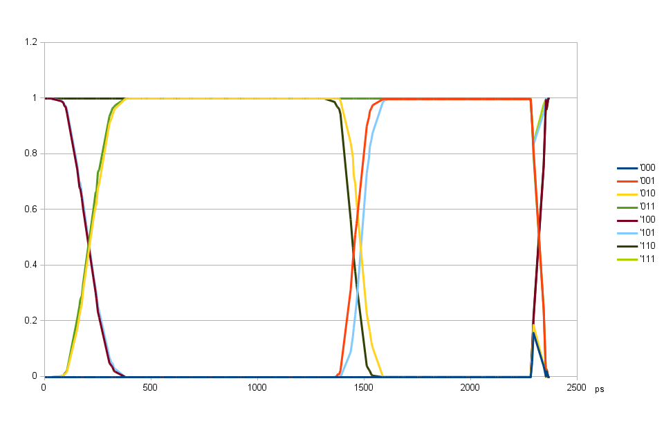
Fig.7. DQ output delays aligned, DQS output delay variable
Scanning over DQS output delays with the individual data bits aligned
When the individual bit output delays are aligned, it is possible to re-scan the eye pattern over variable DQS output delays, the results are shown on Fig. 7. Comparing it with Fig. 5 you may see that improvement is very small, the width of the first transition is virtually the same and on the second transition (around 1500 ps) the individual curves while being “sharper” do not match each other (o10 does not match 110 and 001 does not match 101). This means that there is significant inter-symbol interference (previous bit value influences the next one). There is no split between individual curves around the first transition (~200 ps), but that is just because the history is not followed that far and the result averages both variants, causing the increased width of the individual curves transitions compared to the 1500 ps area. But we used SLEW=”SLOW” for all memory interface outputs in this setup. This it is quite adequate for the 400MHz (800Mb/s) clock rate to reduce the power consumption, but this option will not work when we will increase the clock rate in the future. Then the SLEW=”FAST” will be the only option.
Software Tools Used
This project used various software tools for development.
- Icarus Verilog provided simulation engine. I used the latest version from the Github repository and had to make minor changes to make it work with the project
- GTKWave for viewing simulation results
- Xilinx Vivado and Xilinx ISE WebPack Edition for synthesis, place and route and other implementation tasks. To my personal opinion Xilinx ISE still provides better explanation of what it does during synthesis than newer Vivado, for example – why did it remove some of the register bits. So I was debugging code with ISE first, then later running Vivado tools for the final bitstream generation
- Micron Technology DDR3 SDRAM Verilog Model
- Eclipse IDE (4.3 Kepler) as the development environment to integrate all the other tools
- Python programming language and PyDev – Python development plugin for Eclipse
- VDT plugin for Eclipse (documentation) including the modified version of VEditor. This plugin (currently working for Verilog, tested on GNU Linux and Mac) implements support for Tool Specification Language (TSL) and enables easy integration of the 3rd party tools with support of custom message parsing. I’ll write a separate blog post about this tool, this current eddr3 project is the first one to test VDT plugin in real action.
Fig. 8. VDT plugin screenshot with eddr3 project opened
Conclusions
The eddr3 project demonstrated performance that makes it suitable for Elphel NC393 camera system, successfully implementing DDR3 memory interface to the 512Mx16 device (Micron MT41K256M16HA-107:E) in a single HP34 bank of Xilinx XC7Z030-1FBG484C. The initial data rate equals to the maximal recommended by Xilinx for the hardware setup (using internal Vref) providing 1600MB/s data bandwidth, design uses the SLEW=”SLOW” on all control and data outputs. Evaluation of the performance suggests that it is possible to increase the data rate, probably to above the 3GB/s for the same configuration.
The design was simulated using exclusively Free Software tools without any use of encrypted or undocumented features.
Thanks for posting this. We faced similar difficulties designing with the MIG DDR3 controller and were ultimately not able to use it either. I especially appreciate your mention of the IDELAYE2_FINEDELAY part. I had no idea of it’s existence until I read your post. I think it will help.
Hello,
For our application the DDR3 MIG core has many limitations. Do you think your code could be ported to Ultrascale without a complete rewrite?
Thanks,