DCT type IV implementation
As we finished with the basic camera functionality and tested the first Eyesis4π built with the new 10393 system boards (it is smaller, requires less power and, is faster) we are moving forward with the in-camera image processing. We plan to combine our current camera calibration methods that require off-line post processing and the real-time image correction using the camera own FPGA resources. This project development will require switching between the actual FPGA coding and the software implementation of the same algorithms before going to the next step – software is still easier to design. The first part was in FPGA realm – it was to implement the fundamental image processing block that we already know we’ll be using and see how much of the resources it needs.
Contents
DCT type IV as a building block for in-camera image processing
We consider a small (8×8 pixel) DCT-IV to be a universal block for conditioning of the raw acquired images. Such operations as lens optical aberrations correction, color conversion (de-mosaic) in the presence of the lateral chromatic aberration, image rectification (de-warping) are easier to perform in the frequency domain using convolution-multiplication property and other algorithms.
In post-processing we use DFT (Discrete Fourier Transform) over rather large (64×64 to 512×512) tiles, but that would be too much for the in-camera processing. First is the tile size – for good lenses we do not need that large convolution kernels. Additionally we plan to combine several processing steps into one (based on our off-line post-processing experience) and so we do not need to sub-sample images – in our current software we double resolution of the raw images at the beginning and scale back the final result to reduce image degradation caused by re-sampling.
The second area where we plan to reduce computations is the replacement of the DFT with the DCT that is designed to be fed with the pure real data and so requires less arithmetic operations than DFT that processes complex input values.
Why “type IV” of the DCT?
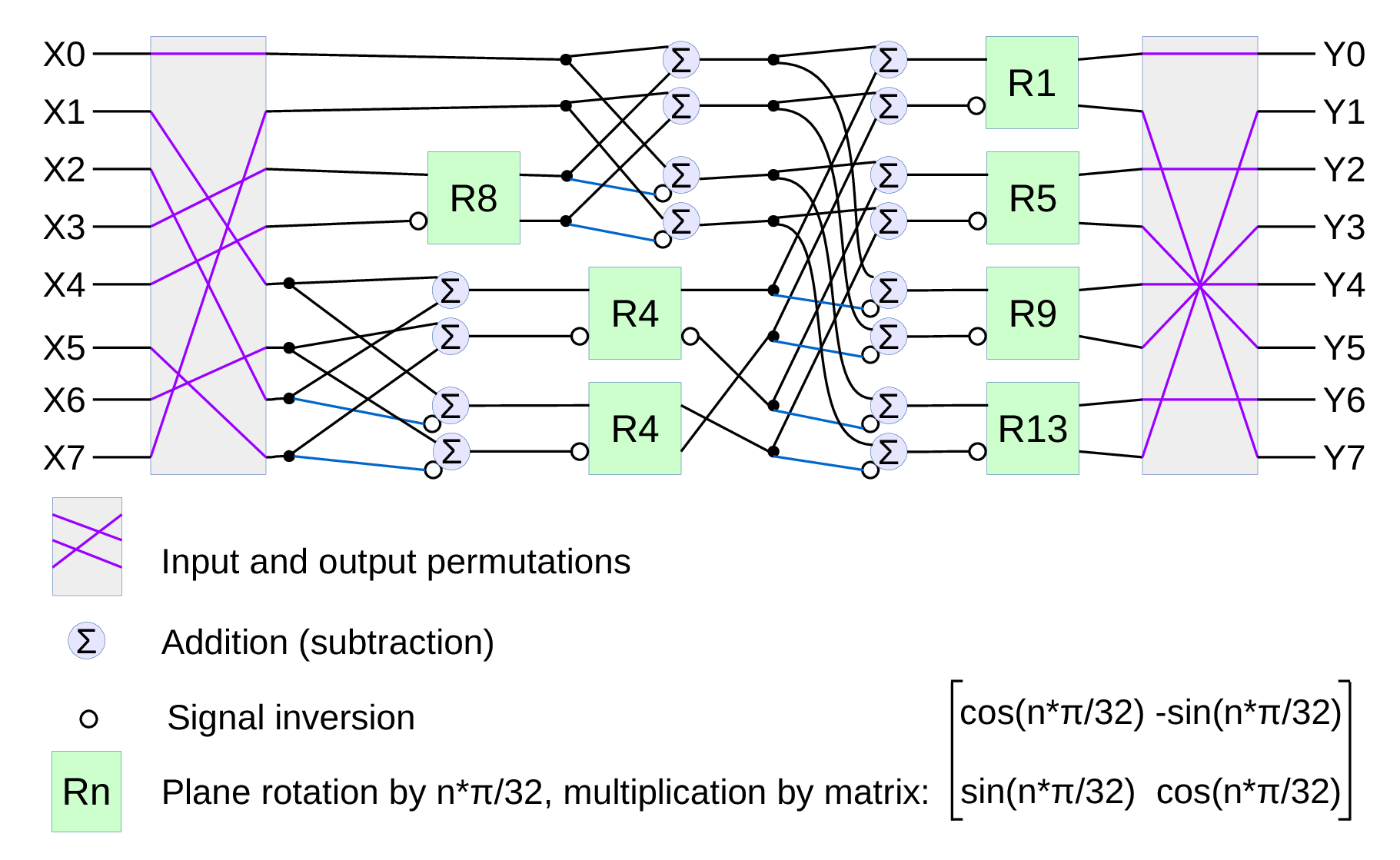
Fig.1. Signal flow graph for DCT-IV
We already have DCT type II implemented for the JPEG/JP4 compression, and we still needed another one. Type IV is used in audio compression because it can be converted to a modified discrete cosine transform (MDCT) – a procedure when multiple overlapped windows are processed one at a time and the results are seamlessly combined without any block artifacts that are familiar for the JPEG with low settings of the compression quality. We too need lapped transform to process large images with relatively small (much smaller than the image itself) convolution kernels, and DCT-IV is a perfect fit. 8-point DCT-IV allows to implement transformation of 16-point segments with 8-point overlap in a reversible manner – the inverse transformation of 8-point data may be converted to 16-point overlapping segments, and being added together these segments result in the original data.
There is a price though to pay for switching from DFT to DCT – the convolution-multiplication property being so straightforward in FFT gets complicated for DCT[1]. While convolving with symmetrical kernels is still simple (just the kernel has to be transformed differently, but it is anyway done off-line in our case), the arbitrary kernel convolution (or just a shift in image space needed to compensate the lateral chromatic aberration) requires both DCT-IV and DST-IV transformed data. DST-IV can be calculated with the same DCT-IV modules (just by reversing the direction of input data and alternating the sign of the output samples), but it still requires additional hardware resources and/or more processing time. Luckily it is only needed for the direct (image domain to frequency domain) transform, the inverse transform IDCT-IV (frequency to image) does not require DST. And IDCT-IV is actually the same as the direct DCT-IV, so we can again instantiate the same module.
Most of the two-dimensional transforms combine 1-d transform modules (because DCT is a separable transform), so we too started with just an 8-point DCT. There are multiple known factorizations for such algorithm[2] and we used one of them (based on BinDCT-IV) shown in Fig.1.
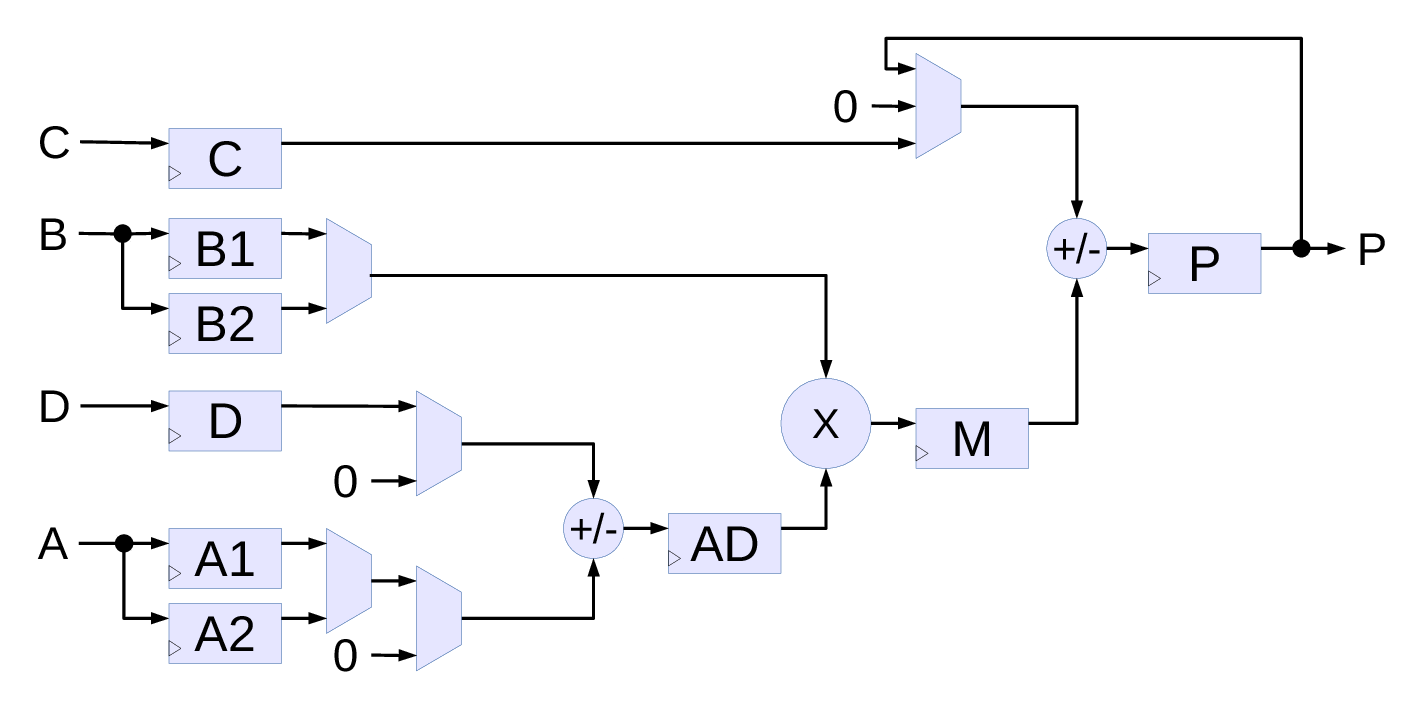
Fig.2. Simplified diagram of Xilinx DSP48E1 primitive (only used functionality is shown)
DSP primitive in Xilinx Zynq
This algorithm is implemented with a pair of DSP48E1[3] primitives shown in Fig.2. This primitive is flexible and allows to configure different functionality, the diagram contains only the blocks and connections used in the current project. The central part is the multiplier (signed 18 bits by signed 25 bits) with inputs from a pair of multiplexed B registers (B1 and B2, 18 bits wide) and the pre-adder AD register (25 bits). The AD register stores sum/difference of the 25-bit D-register and a multiplexed pair of 25-bit A1 and A2 registers. Any of the inputs can be replaced by zero, so AD can receive D, A1, A2, -A1, -A2, D+A1, D-A1, D+A2 and D-A2 values. Result of the multiplier (43 bits) is stored in the M register and the data from M is combined with the 48-bit output accumulator register P. Final adder can add or subtract M to/from one of the P, 48-bit C-register or just 0, so the output P register can receive +/-M, P+/-M and C+/-M. The wrapper module dsp_ma_preadd_c.v reduces the number of DSP48E1 signals and parameters to those required for the project and in addition to the primitive instance have a simple model of the DSP slice to allow simulation without the DSP48E1 source code for convenience.
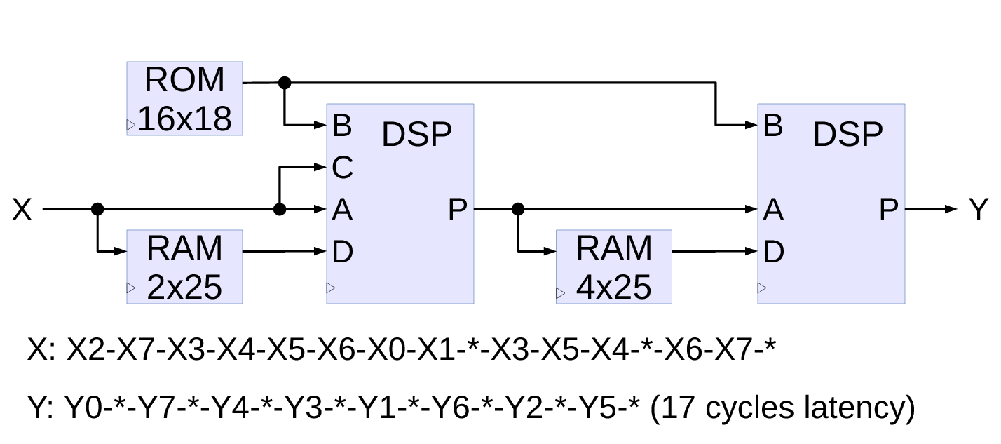
Fig.3. One-dimensional 8-point DCT-IV implementation
8-point DCT-IV transform
The DCT-IV implementation module (Fig.3.) operates in 16 clocks cycles (2 clock periods per data item) and the input/output permutations are not included – they can be absorbed in the data source and destination memories. Current implementation does not implement correct rounding and saturation to save resources – such processing can be added to the outputs after analysis for particular application data widths. This module is not in the coder/decoder signal chain so bit-accuracy is not required.
Data is output each other cycle (so two such modules can easily be used to increase bandwidth), while input data is scrambled more, some of the items have to appear twice in a 16-cycle period. This implementation uses two of the DSP48E1 primitives connected in series. First one implements the left half of the Fig.1. graph – 3 rotators (marked R8, and two of R4), four adders, and four subtracters, The second one corresponds to the right half with R1, R5, R9, R13, four adders, and four subtracters. Two of the small memories (register files) – 2 locations before the first DSP and 4 locations before the second effectively increase the number of the DSP internal D registers. The B inputs of the DSPs receive cosine coefficients, the same ROM provides values for both DSP stages.
The diagram shows just the data paths, all the DSP control signals as well as the memories write and read addresses are generated at the defined times decoded from the 16-cycle period. The decoder is based on the spreadsheet draft of the design.
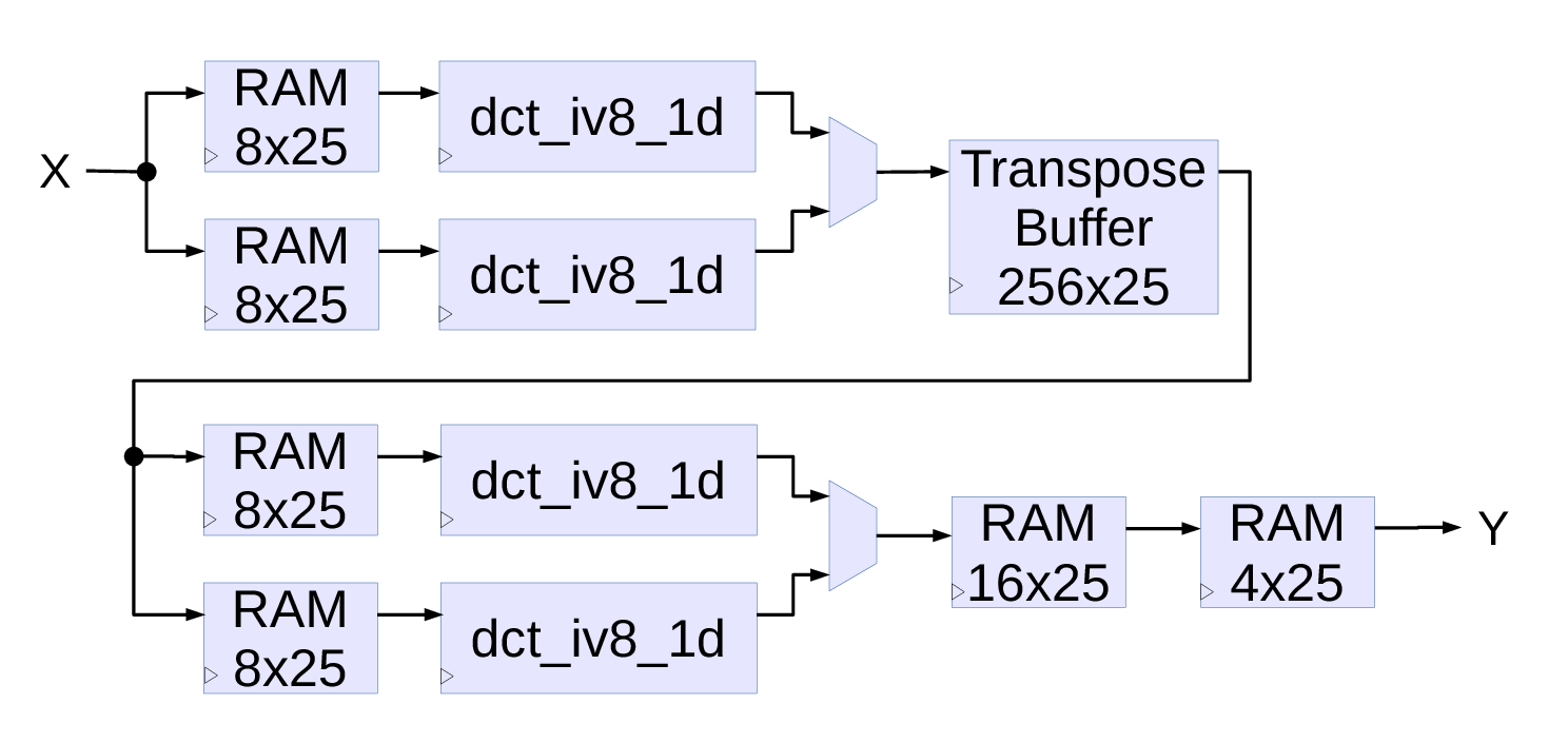
Fig.4. Two-dimensional 8×8 DCT-IV
Two-dimensional 8×8 points DCT-IV
Next diagram Fig.4. shows a two-dimensional DCT type IV implementation using four of the 1-d 8-point DCT-IV modules described above. Input data arrives continuously in line-scan order, next 64-item block may follow either immediately or after a delay of at least 16 cycles so the pipelines phases are correctly restarted. Two of the input 8×25 memories (width can be reduced to match input data, 25 is the width of the DSP48E1 inputs) are used to re-order the input data.As each of the 1-d DCT modules require input data at more than a half cycles (see bottom of Fig.3) interleaving with the common memory for both channels is not possible, so each channel has to have a dedicated one. First of the two DCT modules convert even lines of 8 points, the other one – odd lines. The latency of the data output from the RAM in the second channel is made 1 cycle longer, so the output data from the channels also arrive at odd/even time slots and can be multiplexed to a common transpose buffer memory. Minimal size of the buffer is 2 of the 64 item pages (width can be reduced to match application requirements), but having just a two-page buffer increases the minimal pause time between blocks (if they are not immediate), with a four page buffer (and BRAM primitives are larger even if just halves are used) the minimal non-immediate delay of the 16 cycles of a 1-d module is still valid.
The second (vertical) pass is similar to the first (horizontal) one, it also has individual small memories for input data reordering and 2 output de-scrambler memories. It is possible to use a single stage, but the memory should hold at least 17 items (>16) and the primitives are 16-deep, and I believe that splitting in series makes it easier for the placer/router tools to implement the design.
Next steps
Now when the 8×8 point DCT-IV is designed and simulated the next step is to switch to the Java coding (add to our ImageJ plugin for camera calibration and image post-processing), convert calibration data to the form suitable for the future migration to FPGA and try the processing based on the chosen 8×8 DCT-IV. When satisfied with the results – continue with the FPGA coding.
References
[1] Martucci, Stephen A. “Symmetric convolution and the discrete sine and cosine transforms.” IEEE Transactions on Signal Processing 42.5 (1994): 1038-1051. pdf
[2] Britanak, Vladimir, Patrick C. Yip, and Kamisetty Ramamohan Rao. Discrete cosine and sine transforms: general properties, fast algorithms and integer approximations. Academic Press, 2010.
[3] 7 Series DSP48E1 Slice, UG479 (v1.9), Xilinx, Sep. 2016. pdf
Leave a Reply