AHCI/SATA stack under GNU GPL
Implementation includes AHCI SATA host adapter in Verilog under GNU GPLv3+ and a software driver for GNU/Linux running on Xilinx Zynq. Complete project is simulated with Icarus Verilog, no encrypted modules are required.
This concludes the last major FPGA development step in our race against finished camera parts and boards already arriving to Elphel facility before the NC393 can be shipped to our customers.
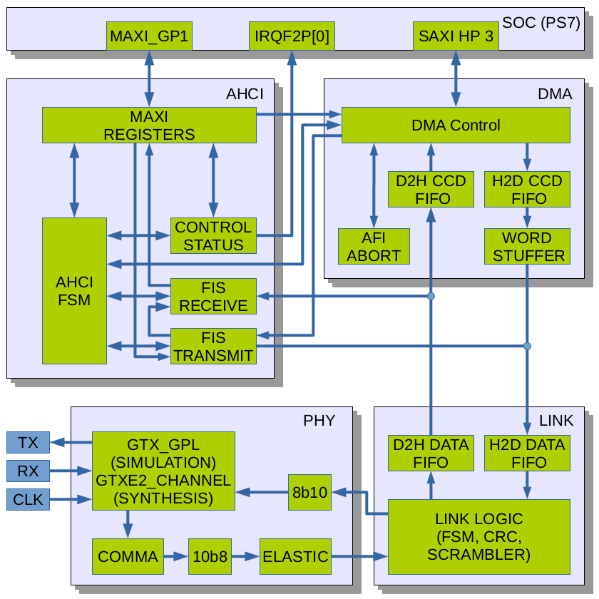
Fig. 1. AHCI Host Adapter block diagram
Contents
Why did we need SATA?
Elphel cameras started as network cameras – devices attached to and controlled over the Ethernet, the previous generations used 100Mbps connection (limited by the SoC hardware), and NC393 uses GigE. But this bandwidth is still not sufficient as many camera applications require high image quality (compared to “raw”) without compression artifacts that are always present (even if not noticeable by the human viewer) with the video codecs. Recording video/images to some storage media is definitely an option and we used it in the older camera too, but the SoC IDE controller limited the recording speed to just 16MB/s. It was about twice more than the 100Mb/s network, but still was a bottleneck for the system in many cases. The NC393 can generate 12 times the pixel rate (4 simultaneous channels instead of a single one, each running 3 times faster) of the NC353 so we need 200MB/s recording speed to keep the same compression quality at the increased maximal frame rate, higher recording rate that the modern SSD are capable of is very desirable.
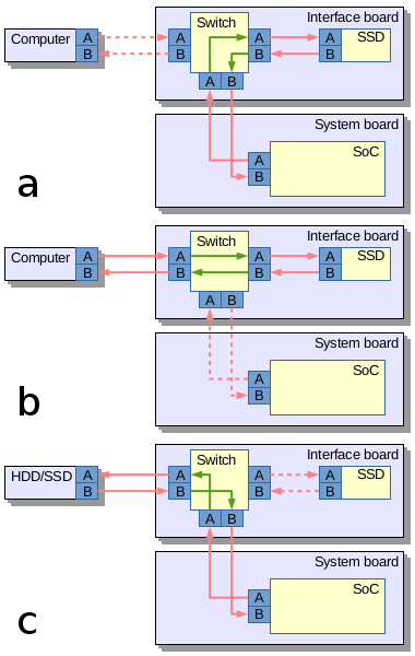
Fig.2. SATA routing: a) Camera records data to the internal SSD; b) Host computer connects directly to the internal SSD; c) Camera records to the external mass storage device
The most universal ways to attach mass storage device to the camera would be USB, SATA and PCIe. USB-2 is too slow, USB-3 is not available in Xilinx Zynq that we use. So what remains are SATA and PCIe. Both interfaces are possible to implement in Zynq, but PCIe (being faster as it uses multiple lanes) is good for the internal storage while SATA (in the form of eSATA) can be used to connect external storage devices too. We may consider adding PCIe capability to boost recording speed, but for initial implementation the SATA seems to be more universal, especially when using a trick we tested in Eyesis series of cameras for fast unloading of the recorded data.
Routing SATA in the camera
It is a solution similar to USB On-The-Go (similar term for SATA is used for unrelated devices), where the same connector is used to interface a smartphone to the host PC (PC is a host, a smartphone – a device) and to connect a keyboard or other device when a phone becomes a host. In contrast to the USB cables the eSATA ones always had identical connectors on both ends so nothing prevented to physically link two computers or two external drives together. As eSATA does not carry power it is safe to do, but nothing will work – two computers will not talk to each other and the storage devices will not be able to copy data between them. One of the reasons is that two signal pairs in SATA cable are uni-directional – pair A is output for the host and input for device, pair B – the opposite.
Camera uses Vitesse (now Microsemi) VSC3304 crosspoint switch (Eyesis uses larger VSC3312) that has a very useful feature – it has reversible I/O ports, so the same physical pins can be configured as inputs or outputs, making it possible to use a single eSATA connector in both host and device mode. Additionally VSC3304 allows to change the output signal level (eSATA requires higher swing than the internal SATA) and perform analog signal correction on both inputs and outputs facilitating maintaining signal integrity between attached SATA devices.
Aren’t SATA implementations for Xilinx Zynq already available?
Yes and no. When starting the NC393 development I contacted Ashwin Mendon who already had SATA-2 working on Xilinx Virtex. The code is available on OpenCores under GNU GPL license. There is an article published by IEEE . The article turned out to be very useful for our work, but the code itself had to be mostly re-written – it was still for different hardware and were not able to simulate the core as it depends on Xilinx proprietary encrypted primitives – a feature not compatible with the free software simulators we use.
Other implementations we could find (including complete commercial solution for Xilinx Zynq) have licenses not compatible with the GNU GPLv3+, and as the FPGA code is “compiled” to a single “binary” (bitstream file) it is not possible to mix free and proprietary code in the same design.
Implementation
The SATA host adapter is implemented for Elphel NC393 camera, 10393 system board documentation is on our wiki page. The Verilog code is hosted at GitHub, the GNU/Linux driver ahci_elphel.c is also there (it is the only hardware-specific driver file required). The repository contains a complete setup for simulation with Icarus Verilog and synthesis/implementation with Xilinx tools as a VDT (plugin for Eclipse IDE) project.
Current limitations
The current project was designed to be a minimal useful implementation with provisions to future enhancements. Here is the list of what is not yet done:
- It is only SATA2 (3GHz) while the hardware is SATA3(6GHz) capable. We will definitely work on the SATA3 after we will complete migration to the new camera platform. Most of the project modules are already designed for the higher data rate.
- No scrambling of outgoing primitives, only recognizing incoming ones. Generation of CONTp is optional by SATA standard, but we will definitely add this as it reduces EMI and we already implemented multiple hardware measures in this direction. Most likely we will need it for the CE certification.
- No FIS-based switching for port multipliers.
- Single command slot, and no NCQ. This functionality is optional in AHCI, but it will be added – not much is missing in the current design.
- No power management. We will look for the best way to handle it as some of the hardware control (like DevSleep) requires i2c communication with the interface board, not directly under FPGA control. Same with the crosspoint switch.
There is also a deviation from the AHCI standard that I first considered temporary but now think it will stay this way. AHCI specifies that a Command list structure (array of 32 8-DWORD command headers) and a 256-byte Received FIS structure are stored in the system memory. On the other hand these structures need non-paged memory, are rather small and require access from both CPU and the hardware. In x393_sata these structures are mapped to the register memory (stored in the FPGA RAM blocks) – not to the regular system memory. When working with the AHCI driver we noticed that it is even simpler to do it that way. The command tables themselves that involve more data passing form the software to device (especially PRDT – physical region descriptor tables generated from the scatter-gather lists of allocated data memory) are stored in the system memory as required and are read to the hardware by the DMA engine of the controller.
As of today the code is still not yet cleaned up from temporary debug additions. It will all be done in the next couple weeks as we need to combine this code with the large camera-specific code – SATA controller (~6% of the FPGA resources) was developed separately from the rest of the code (~80% resources) as it makes both simulation and synthesis iterations much faster.
Extras
This implementation includes some additions functionality controlled by Verilog `ifdef directives. Two full block RAM primitives as used for capturing data in the controller. One of these “datascopes” captures incoming data right after 10b/8b decoder – it can store either 1024 samples of the incoming data combined of 16 bit of data plus attributes or the compact form when each 32-bit primitive is decoded and the result is a 5-bit primitive/error number. In that case 6*1024 primitives are recorded – 3 times longer than the longest FIS.
Another 4KB memory block is used for profiling – the controller timestamps and records first 5 DWORDs of each each incoming and outgoing FIS, additionally it timestamps software writes to the specific location allowing mixed software/hardware profiling.
This project implements run-time access to the primitive attributes using Xilinx DRP port of the GTX elements, same interface is used to programmatically change the logical values of the configuration inputs, making it significantly simpler to guess how the partially documented attributes change the device functionality. We will definitely need it when upgrading to SATA3.
Code description
Top connections
The controller uses 3 differential I/O pads of the device – one input pair (RX on Fig.1) and one output pair (TX) make up a SATA port, additional dedicated input pair (CLK) provides 150MHz that synchronizes most of the controller and the transmit channel of the Zynq GTX module. In the 10393 board uses SI53338 spread-spectrum capable programmable clock to drive this input.
Xilinx conventions tell that the top level module should instantiate the SoC Processing System PS7 (I would consider connections to the PS7 as I/O ports), so the top module does exactly that and connects to AXI ports of the actual design top module to the MAXIGP1 and SAXIHP3 ports of the PS7, IRQF2P[0] provides interrupt signal to the CPU. MAXIGP1 is one of the two 32-bit AXI ports where CPU is master – it is used for PIO access to the controller register memory (and read out debug information), SAXIHP3 is one of the 4 “high performance” 64-bit wide paths, this port is used by the controller DMA engine to transfer command tables and data to/from the device. The port numbers are selected to match ones unused in the camera specific code, other designs may have different assignments.
Clocks and clock domains
Current SATA2 implementation uses 4 different clock domains, some may be shared with other unrelated modules or have the same source.
- aclk is used in MAXIGP1 channel and part of the MAXI REGISTERS module synchronizing AXI-pointing port of the dual-port block RAM that implements controller registers. 150 MHz (maximal permitted frequency) is used, it is generated from one of the PS7 FPGA clocks
- hclk is used in AXI HP3 channel, DMA Control and parts of the H2D CCD FIFO (host-to-device cross clock domain FIFO ), D2H CCD FIFO and AFI ABORT modules synchronizing. 150 MHz (maximal permitted frequency) is used, same as the aclk
- mclk is used throughout most of the other modules of the controller except parts of the GTX, COMMA, 10b8 and input parts of the ELASTIC. For current SATA2 implementation it is 75MHz, this clock is derived from the external clock input and is not synchronous with the first two
- xclk – source-synchronous clock extracted from the incoming SATA data. It drives COMMA and 10b8 modules, ELASTIC allows data to cross clock boundaries by adding/removing ALIGNp primitives
ahci_sata_layers
The two lower layers of the stack (phy and link) that are independent of the controller system interface (AHCI) are instantiated in ahci_sata_layers.v module together with the 2 FIFO buffers for D2H (incoming) and H2D outgoing data.
SATA PHY
SATA PHY layer Contains the OOB (Out Of Band) state machine responsible for handling COMRESET,COMINIT and COMWAKE signals, the rest is just a wrapper for the functionality of the Xilinx GTX transceiver. This device includes both high-speed elements and some blocks that can be synthesized using FPGA fabric. Xilinx does not provide the source code for the GTX simulation module and we were not able to match the hardware operation to the documentation, so in the current design we use only those parts of the GTXE2_CHANNEL primitive that can not be replaced by the fabric. Other modules are implemented as regular Verilog code included in the x393_sata project. There is a gtx_wrap module in the design that has the same input/output ports as the primitive allowing to select which features are handled by the primitive and which – by the Verilog code without changing the rest of the design.
The GTX primitive itself can not be simulated with the tools we use, so the simulation module was replaced, and Verilog `ifdef directive switches between the simulation model and non-free primitive for synthesis. The same approach we used earlier with other Xilinx proprietary primitives.
Link
Link module implements SATA link state machine, scrambling/descrambling of the data, calculates CRC for transmitted data and verifies CRC for the received one. SATA does not transmit and receive data simultaneously (only control primitives), so both CRC and scrambler modules have a single instance each providing dual functionality. This module required most troubleshooting and modifications during testing the hardware with different SSD – at some stages controller worked with some of them, but not with others.
ahci_top
Other modules of the design are included in the ahci_top. Of them the largest is the DMA engine shown as a separate block on the Fig.1.
DMA
DMA engine makes use of one of the Zynq 64-bit AXI HP ports. This channel includes FIFO buffers on the data and address subchannels (4 total) – that makes interfacing rather simple. The hard task is resetting the channels after failed communication of the controller with the device – even reloading bitsteam and resetting the FPGA would not help (actually it makes things even worse). I searched Xilinx support forum and found that similar questions where only discussed between the users, there was no authoritative recommendation from Xilinx staff. I added axi_hp_abort module that watches over the I/O transactions and keeps track of what was sent to the FIFO buffers, being able to complete transactions and drain buffers when requested.
The DMA module reads command table, saves command data in the memory block to be later read by the FIS TRANSMIT module, it then reads the scatter-gather memory descriptors (PRDT) (supporting pre-fetch if enabled) and reads/writes the data itself combining the fragments.
On the controller side data that comes out towards the device (H2D CCD FIFO) and coming from device(D2H CCD FIFO) needs to cross the clock boundary between hclk and mclk, and handle alignment issues. AXI HP operates in 64-bit mode, data to/from the link layer is 32-bit wide and AHCI allows alignment to the even number of bytes (16bits). When reading from the device the cross-clock domain FIFO module does it in a single step, combining 32-bit incoming DWORDs into 64-bit ones and using a barrel shifter (with 16-bit granularity) to align data to the 64-bit memory QWORDs – the AXI HP channel provides per-byte write mask that makes it rather easy. The H2D data is converted in 2 steps: First it crosses the clock domain boundary being simultaneously transformed to 32-bit with a 2-bit word mask that tells which of the two words in each DWORD are valid. Additional module WORD STUFFER operates in mclk domain and consolidates incoming sparse DWORDs into full outgoing DWORDs to be sent to the link layer.
AHCI
The rest of the ahci_top module is shown as AHCI block. AHCI standard specifies multiple registers and register groups that HBA has. It is intended to be used for PCI devices, but the same registers can be used even when no PCI bus is physically present. The base address is programmed differently, but the relative register addressing is still the same.
MAXI REGISTERS
MAXI REGISTERS module provides the register functionality and allows data to cross the clock domain boundary. The register memory is made of a dual-port block RAM module, additional block RAM (used as ROM) is pre-initialized to make each bit field of the register bank RW (read/write), RO (read only), RWC (read, write 1 to clear) or RW1 (read, write 1 to set) as specified by the AHCI. Such initialization is handled by the Python program create_ahci_registers.py that also generates ahci_localparams.vh include file that provides symbolic names for addressing register fields in Verilog code of other modules and in simulation test benches. The same file runs in the camera to allow access to the hardware registers by names.
Each write access to the register space generates write event that crosses the clock boundary and reaches the HBA logic, it is also used to start the AHCI FSM even if it is in reset state.
The second port of the register memory operates in mclk domain and allows register reads and writes by other AHCI submodules (FIS RECEIVE – writes registers, FIS TRANSMIT and CONTROL STATUS)
The same module also provides access to debug registers and allows reading of the “datascope” acquired data.
CONTROL STATUS
The control/status module maintains “live” registers/bits that the controller need to react when they are changed by the software and react on various events in the different parts of the controller. The updated register values are written to the software accessible register bank.
This module generates interrupt request to the processor as specified in the AHCI standard. It uses one of the interrupt lines from the FPGA to the CPU (IRQF2P) available in Zynq.
AHCI FSM
The AHCI state machine implements the AHCI layer using programmable sequencer. Each state traverses the following two stages: actions and conditions. The first stage triggers single-cycle pulses that are distributed to appropriate modules (currently 52 total). Some actions require just one cycle, others wait for “done” response from the destination. Conditions phase involves freezing logical conditions (now 44 total) and then going through them in the order specified in AHCI documentation. The state description for the machine is provided in the Assembler-like format inside the Python program ahci_fsm_sequence.py it generates Verilog code for the action_decoder.v and condition_mux.v modules that are instantiated in the ahci_fsm.v.
The output listing of the FSM generator is saved to ahci_fsm_sequence.lst. Debug output registers include address of the last FSM transition, so this listing can be used to locate problems during hardware testing. It is possible to update the generated FSM sequence at run time using designated as vendor-specific registers in the controller I/O space.
FIS RECEIVE
The FIS RECEIVE module processes incoming FIS (DMA Setup FIS, PIO Setup FIS, D2H register FIS, Set device bits FIS, unknown FIS), updates required registers and saves them in the appropriate areas of received FIS structure. For incoming data FIS it consumes just the header DWORD and redirects the rest to the D2H CCD FIFO of the DMA module. This module also implements the word counters (PRD byte count and decrementing transfer counter), these counters are shared with the transmit channel.
FIS TRANSMIT
FIS TRANSMIT module recognizes the following commands received from the AHCI FSM: fetch_cmd, cfis_xmit, atapi_xmit and dx_xmit, following the prefetch condition bit. The first command (fetch_cmd) requests DMA engine to read in the command table and optionally to prefetch PRD memory descriptors. The command data is read from the DMA module memory after one of the cfis_xmit or atapi_xmit comamnds, it is then transmitted to the link layer to be sent to device. When processing the dx_xmit this module sends just the header DWORD and transfers control to the DMA engine, continuing to count PRD byte count and decrementing transfer counter.
FPGA resources used
According to the “report_utilization” Xilinx Vivado command, current design uses:
- 1358 (6.91%) slices
- 9.5 (3.58%) Block RAM tiles
- 7 (21.88%) BUFGCTRL
- 2 (40%) PLLE2_ADV
The resource usage will be reduced as there are debug features not yet disabled. One of the PLLE2_ADV uses clock already available in the rest of the x393 code (150MHz for MAXIGP1 and SXAHIHP3), the other PLL that produces 75MHz transmit-synchronous clock can probably be eliminated too. Two of the block RAM tiles are capturing incoming primitives and profiling data, this functionality is not needed in the production version. More the resources may be saved if we’ll be able to use the hard-wired 10b/8b decoder, 8b/10b encoder, comma alignment and elastic buffer primitives of the Xilinx GTXE2_CHANNEL.
Update: eliminated use of the PLLE2_ADV in the SATA controller (one left is just to generate AXI clock, it is not needed with proper setting of the PS output clock), reduced number of slices (datascope functionality preserved) to 1304 (6.64%). PLLs are valuable resource for multi-sensor camera as we keep possibility to use different sensors/clocks on each sensor port.
Testing the hardware
Testing with Python programs
All the initial work with the actual hardware was done with the Python script that started with reimplementation of the same functionality used when simulating the project. Most is in x393sata.py that imports x393_vsc3304.py to control the VSC3304 crosspoint switch. This option turned out very useful for troubleshooting starting from initial testing of the SSD connection (switch can route the SSD to the desktop computer), then for verifying the OOB exchange (the only what is visible on my oscilloscope) – switch was set to connect SSD to Zynq, and use eSATA connector pins to duplicate signals between devices, so probing did not change the electrical characteristics of the active lines. Python program allowed to detect communication errors, modify GTX attributes over DRP, capture incoming data to reproduce similar conditions with the simulator. Step-by-step it was possible to receive signature FIS, then get then run the identify command. In these tests I used large area of the system memory that was reserved as a video ring buffer set up as “coherent” DMA memory. We were not able to make it really “coherent” – the command data transmitted to the device (controller reads it from the system memory as a master) often contained just zeros as the real data written by the CPU got stuck in either one of the caches or in the DDR memory controller write buffer. These errors only went away when we abandoned the use of the coherent memory allocation and switched to the stream DMA with explicit synchronization with dma_sync_*_for_cpu/dma_sync_*_for_device.
AHCI driver for GNU/Linux
Mikhail Karpenko is preparing post about the software driver, and as expected this development stage revealed new controller errors that were not detected with just manual launching commands through the Python program. When we mounted the SSD and started to copy gigabyte files, the controller reported some fake CRC errors. And it happened with one SSD, but not with the other. Using data capturing modules it was not so difficult to catch the conditions that caused errors and then reproduce them with the simulator – one of the last bugs detected was that link layer incorrectly handled single incoming HOLD primitives (rather unlikely condition).
Performance results
First performance testing turned out to be rather discouraging – ‘dd’ reported under 100 MB/s rate. At that point I added profiling code to the controller, and the data rate for the raw transfers (I tried command that involved reading of 24 of the 8KB FISes), measured from the sending of the command FIS to the receiving of the D2H register FIS confirming the transfer was 198MB/s – about 80% of the maximal for the SATA2. Profiling the higher levels of the software we noticed that there is virtually no overlap between the hardware and software operation. It is definitely possible to improve the result, but the fact that the software slowed twice the operation tells that it if the requests and their processing were done in parallel, it will consume 100% of the CPU power. Yes, there are two cores and the clock frequency can be increased (the current boards use the speed grade 2 Zynq, while the software still thinks it is speed grade 1 for compatibility with the first prototype), it still may be a big waste in the camera. So we will likely bypass the file system for sequential recording video/images and use the second partition of the SSD for raw recording, especially as we will record directly from the video buffer of the system memory, so no dealing with scatter-gather descriptors, and no need to synchronize system memory as no cache is involved. The memory controller is documented as being self-coherent, so reading the same memory while it is being written to through a different channel should cause write operation to be performed first.
Conclusions and future plans
We’ve achieved the useful functionality of the camera SATA controller allowing recording to the internal high capacity m.2 SSD, so all the hardware is tested and cameras can be shipped to the users. The future upgrades (including SATA3) will be released in the same way as other camera software. On the software side we will first need to upgrade our camogm recorder to reduce CPU usage during recording and provide 100% load to the SATA controller (rather easy when recording continuous memory buffer). Later (it will be more important after SATA3 implementation) we may optimize controller even more try to short-cut the video compressors outputs directly to the SATA controller, using the system memory as a buffer only when the SSD is not ready to receive data (they do take “timeouts”).
We hope that this project will be useful for other developers who are interested in Free Software solutions and prefer the Real Verilog Code (RVC) to all those “wizards”, “black boxes” and “IP”.
Software tools used (and not)
Elphel designs and builds high performance cameras striving to provide our users/developers with the design freedom at every possible level. We do not use any binary-only modules or other hidden information in our designs – all what we know ourselves is posted online – usually on GitHub and Elphel Wiki. When developing FPGA, and that unfortunately still depends on proprietary tools, we limit ourselves to use only free for download tools to be exactly in the same position as many of our users. We can not make it necessary for the users (and consider it immoral) to purchase expensive tools to be able to modify the free software code for the hardware they purchased from Elphel, so no “Chipscopes” or other fancy proprietary tools were used in this project development.
Keeping information free is a precondition, but it is not sufficient alone for many users to be able to effectively develop new functionality to the products, there needs to be ease of doing that. In the area of the FPGA design (and it is a very powerful tool resulting in high performance that is not possible with just software applications) we think of our users as smart people, but not necessarily professional FPGA developers. Like ourselves.
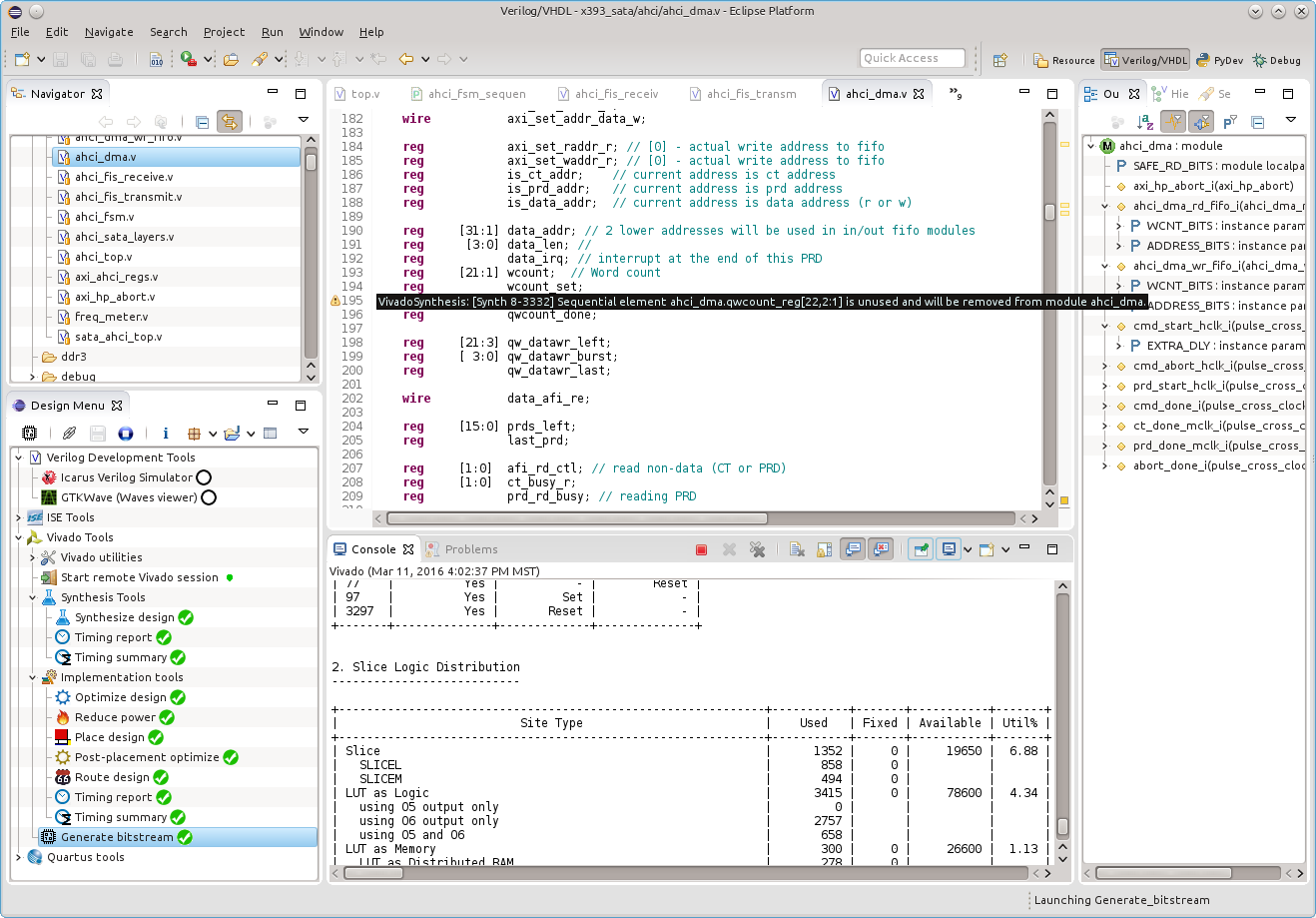
Fig.3 FPGA development with VDT
We learned a lesson from our previous FPGA projects that depended too much on particular releases of Xilinx tools and were difficult to maintain even for ourselves. Our current code is easier to use, port and support, we tried to minimize dependence on particular tools used what we think is a better development environment. I believe that the “Lego blocks” style is not the the most productive way to develop the FPGA projects, and it is definitely not the only one possible.
Treating HDL code similar to the software one is not less powerful paradigm, and to my opinion the development tools should not pretend to be “wizards” who know better than me what I am allowed (or not allowed) to do, but more like gentle secretaries or helpers who can take over much of routine work, remind about important events and provide some appropriate suggestions (when asked for). Such behavior is even more important if the particular activity is not the only one you do and you may come back to it after a long break. A good IDE should be like that – help you to navigate the code, catch problems early, be useful with default settings but provide capabilities to fine tune the functionality according to the personal preferences. It is also important to provide familiar environment, this is why we use the same Eclipse IDE for Verilog, Python, C/C++ and Java and more. All our projects come with the initial project settings files that can be imported in this IDE (supplemented by the appropriate plugins) so you can immediately start development from the point we currently left it.
For FPGA development Elphel provides VDT – a powerful tool that includes deep Verilog support and integrates free software simulator Icarus Verilog with the Github repository and a popular GTKWave for visualizing simulation results. It comes with the precofigured support of FPGA vendors proprietary synthesis and implementation tools and allows addition of other tools without requirement to modify the plugin code. The SATA project uses Xilinx Vivado command line tools (not Vivado GUI), support for several other FPGA tools is also available.
Hi
I love your blogs, very informative.
Just thought you know the AROS community have set up projects for qualified professionals to earn some pocket change :
https://power2people.org/projects/ahci/
community
http://aros-exec.org/
I think you may enjoy this challenge.
Missing projects can easily be added /changed in stages.
Also the Apollo crew are working on an FPGA based Amiga system – drop in and say hello.
http://www.apollo-core.com/knowledge.php