NC393 development progress
Development of the NC393 is now started, at last – last 6 weeks I’m working on it full time. It is still a long way ahead before the new camera will replace our current model 353, but at least the very first step is completed – I just finished the PCB layout of the system board.
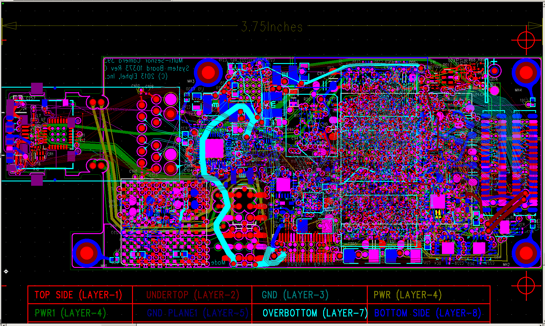
10393 System Board PCB layout
There were not so many changes to the specs/features that were planned and described in the October 2012 post, the camera will be powered by Xilinx Zynq SoC (XC7Z030-1FBG484C to be exact) that combines high performance FPGA with a dual ARM CPU and generous set of built-in peripherals. It will have 1GB of on-board system memory and 512MB of additional dedicated video/FPGA memory (the NC353 has 64MB each of them). Both types of memory consist of the same 256Mx16 DDR3 chips – 2 for the system (to use full available memory bus width of 32 bits) and one for the FPGA.
The main class of the camera applications remains to be a multi-sensor. Even more so – the smallest package of the Zynq 7030 device turned out to have sufficient number of I/Os to accommodate 4 sensor ports – originally I planned only 3 of them. These sensor ports are fully compatible with our current 5MPix sensor boards and with the existent 10359 sensor multiplexer boards – with such multiplexers it will be possible to control up to 12 sensors with a single 10393. Four of the connectors are placed in two pairs on both sides of the PCB, so they overlap on the layout image.
These 5MPix Aptina sensors have large (by the modern standards) pixels with the pitch of 2.2 microns and that, combined with good quality of the sensor electronics will keep them useful for many of the applications in the future. This backward compatibility will allow us to reduce the amount of hardware needed to be redesigned simultaneously, but of course we are planning to use newer sensors – both existent and those that might be released in the next few years. Thanks to FPGA flexibility, the same sensor board connectors will be able to run alternative types of signals having programmable voltage levels – this will allow us to keep the same camera core current for the years to come.
Alternative signals are designed to support serial links with differential signals common in the modern sensors. Each of the connectors can use up 8 lanes plus differential clock, plus I²C and an extra pair of control signals. These four connectors use two FPGA I/O banks (two per bank), each bank has run-time programmable supply voltage to accommodate variety of the sensor signal levels.
We plan to hold the 10393 files for about a month before releasing them into production of the prototype batch while I will develop the two companion boards. Not very likely, but the development of these additional boards may lead to some last-minute changes to the system board.
One of them – 10389 will have functionality similar to the current 19369 board – it will provide mass storage (using mSATA SSD), inter-camera synchronization (so we will be able to use these camera modules in Eyesis4π cameras) and back panel I/O connectors, including microUSB, eSATA/USB combo and synchronization in/out. The eSATA/USB combo connector will allow attaching the external storage devices powered by the camera. The same eSATA port will be reconfigurable into the slave mode, so the images/video recorded to the internal mSATA SSD will be transferred to the host computer significantly faster than the main GigE network port allows.
Another board to develop (10385) is the power supply – I decided to remove the primary DC-DC converter from the system board. Camera uses multiple DC-DC converters – even the processor alone needs several voltage rails, but internally it uses a single regulated 3.3V – all the other (secondary) converters use 3.3V as their input and provide all the other voltages needed. In the 10393 boards most secondary voltages are programmable making it possible to implement “margining” – testing the camera at lower and higher than nominal voltage and making sure it can reliably withstand such variations and is not operating on the very edge of the failure during the production testing. Primary power supply role is to provide a single regulated voltage starting form different sources such as power over the network, battery, wall adapter or some other source. It may need to be isolated or not, the input power quality may be different.
One reason to separate the primary power supply from the system board is that currently we have about half of the cameras made to be powered over the network, and another half – modified to use lower voltege from the batteries. Currently we order the 10353 boards without any DC-DC converter and later install one of the two types of the converters and make other small changes on the board. Some of our customers do not need any of the primary DC-DC converters – they embed the 10353 boards and provide regulated 3.3V to the modified 10353 board directly. Multi-camera systems can also share primary power supplies. This makes it more convenient to make a power supply as a plug-in module, so the system board itself can be finished in one run.
Another reason to remove the primary power from the system board is to remove the IEEE 802.3af (PoE) functionality. During the several last years we survived multiple attacks of the “patent trolls” (or NPE – non-practicing entities, how they like to call themselves), but we’ve spent thousands of dollars paid to the lawyers to deal with the trolls – some of the them tried to sell us the license for the already expired patents. One of the still active patents is related to “phantom power “- providing power through the signal lines, similar to how it is done for the microphones since 1919. To avoid the attacks of the trolls in the 10353 cameras we were able to use power over the spare pairs (Alternative B), but that is not possible with GigE which needs all 4 pairs in a cable. We do not believe that using this nearly century-old technology constitutes a genuine invention (maybe tomorrow somebody will “invent” powering SATA devices in the same way? Or already did?) but being a small company we do not have the power to fight in this field and invalidate those patents.
So the new NC393 made by Elphel will not have the PoE functionality, we will not make, manufacture, sell or market it (at least in GigE mode). But the camera will be PoE-ready, so as soon as the patent will become invalid, it will be possible to add the functionality by just replacing the plug-in module. And of course our cameras are open and hackable, so our users (in the countries where it is legal, of course – similar to installation of some of the software programs) will be able to build and add such module to their cameras without us.
Both of these companion boards are already partially designed so I plan that next month we will be able to release the files to production and start building the first prototype system. To test the basic functionality of the system board the two other ones are not needed – serial debug port (with the embedded USB-to-serial converter) is located on the system board, and 3.3V will be anyway originally provided by a controlled power supply. When everything will be put together the camera will get a well-known but still a nice feature for the autonomous battery-powered timelapse imaging: it will be able to wake itself up (using alarm signal from the internal clock/calendar that it has anyway), boot, capture some images and turn the power off virtually completely – until the next alarm.
That is some exciting progress! Do you have any feeling at this point how much of the FPGA will be left for other algorithms? Do you have a prediction on CPU usage at maximum camera bandwidth?
Hi Lee, I believe there will be plenty of room left after implementation of the basic functionality we had in 353. Even if we multiply the resources by 4 (per number of sensor channels) it will still leave plenty. Current utilization in the 353 camera with spartan3E (http://elphel.cvs.sourceforge.net/viewvc/elphel/elphel353-8.0/fpga/x3x3/x353.par?view=markup )
Number of MULT18X18SIOs 19 out of 28 67%
Number of RAMB16s 22 out of 28 78%
Number of Slices 7247 out of 8672 83%
7030 has 265 Block RAMs, 400 DSP slices, 78600 LUTs/157200 FFs
I will know that better when will start a real FPGA work – first there will be the memory controller to replace the generic one from Xilinx. With CPU usage – I also do not have any specific estimations yet, but I do not expect it to be a bottleneck when using the FPGA processing. The main problem with DaVinci that caused me to abandon 373 (FPGA to CPU/system memory bandwidth) is not a problem with Zynq, and there I will still use a separate DDR3 memory for the FPGA, so system memory bandwidth will not have much of the FPGA load – just writing the results.
Andrey
Interesting layout. What CAD software are you using?
Hi Brody, I wold like not to advertise proprietary tools, and this one is a ~15 year old program running on Wine. The board is rather small so all routing is done manually. I will be really happy when it will be possible for us to use (and write about) Free tools, like Kicad. I hope it will happeng soon as Kicad is now supported by CERN – http://cernandsociety.web.cern.ch/technology/kicad-development (and we can do that too).
Hi Andrey; nice to hear some news !
Will you consider adding an interface for accessing the JPEG compressed or bayer streams over V4L2 on the Linux system running on the ARM core ? It would enable third party developers to use the existing NEON-optimized encoders e.g. VP8, theorarm, …
Florent, yes that will most likely happen. The focus of the new camera FPGA processing will be real-time image processing, not the image compression. And compression will be handled in the way you suggested.
Andrey
Hi. Are you only using 8 layers for your board with the Zynq chip on it? Is do are you using blind/buried vias? The reason I ask is that I am working on a board with the 7030 chip and I am struggling to route it using only 8 layers.
Jon, yes we do use both blind and buried vias (on 8 layers) as we have memory chips just opposite of the 7030 chip, there are microvias 1-2, 7-8 and buried 2-7. We will post documentation after the prototypes will be tested and we’ll start shipping the actual cameras to the users.
Здравствуйте, Андрей. На просторах интернета набрел на ваш сайт и заинтересовался разведенной вами платой в автотрассировщике Топор. Используете ли вы Топор сейчас в своих разработках? Сложно ли его настраивать при трассировке БГА компонентов и большого числа диффпар? Сам работая в Altium Designer, но пробовал топор. Не понравилось, что нужно очень много правил задавать.
Hello Anton, I’ve never used TopoR myself, but you are not the first to think we did :-). All our PCBs are routed manually using some 15-year old software that I was able to run on Wine. I did try Altium 3 years ago, but it had many problems running on Wine and it is a must for us. We are now trying to switch to KiCAD but so far it misses too many of the features that are critical for us.
Andrey