September 29, 2009
by Oleg Dzhimiev
The modes are:
- Direct alternating channels mode.
At first, I rewrote the logic of switching from what I already had and this resulted in parsedit.php “Error 500” and the streamer stop (when the sensors were in the free run mode, in triggered – everything was ok) while it was everything fine with the testbench. Coudn’t find what is wrong for sometime. Part of the logic was based on sync signals levels and under certain conditions the switching didn’t work – the error was corrected by using only the sync signals edges.
 Fig.1 A sample frame in the testbench is 2592×3 (to reduce verification time), “ivact” – vertical sync signal, “ihact” – horizontal sync signal, “pxdr” – pixel data. White numbers in ‘ivact’ line represent an appropriate channel.
- Alternating channels – one channel direct, another – bufferred.
With this mode the situation was almost the same as with the previous mode – the same changes but the frame from the second channel, the one that is buffered looks brighter, but if to disable the first channel – the buffered frame is correct:
 Fig.2 “framen” – frame enable register, allows work when ‘high’.

Fig.3 Good direct frame (left) and ‘whitened’ buffered frame (right). Probably some signal’s latencies are incorrect.
Is separate due to the problems with other two modes. It’s being added currently.
I’m also making the project less messy, optimizing registers addresses and rewriting scripts to make the work with 10359 easier.
September 24, 2009
by Andrey Filippov
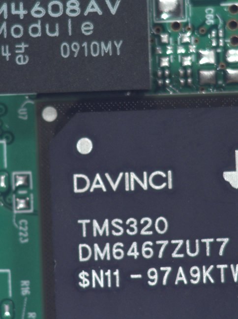
10373A with BGA chips installed - fragment
Finally I received the 10373A PCB with BGA chips soldered. Still one (DDR3 for the video memory) is missing, we’ll install it later – anyway there is a lot to be done before I’ll need it. But that’s all what is soldered for me – I could not do it by hand. Hundreds of other components are waiting for me – I attached two of the model 353 cameras as microscopes and prepared to solder 0201 resistors and capacitors (0.3mm by 0.6mm) – I’ve never done it before. It may be stupid to try to do that manually, but it did work for me before to use a soldering iron after working with just virtual stuff on the computer. I believe it helps me to find some potential problems in the design while I take components one by one and think of them in different perspective than during the initial design.
And while I was waiting for the components and the board – I made some minor design upgrades to the existent camera – changed the layout of the sensor board to fit better multi-sensor applications (like panoramic video). The new board is just 15mm by 28mm (current 10338 is 32mm x 32mm), so using M12 (S-mount) lenses it is possible to shrink the size of the panoramic head so the distance between the outer elements of the opposite lenses is under 80mm – it is much smaller than similar high-res systems. That distance is important to reduce parallax – most noticable when the objects are close to the camera.
September 7, 2009
by Andrey Filippov
In September 2009 there were multiple publications about the Open Source Frankencamera developed at Stanford (Open-source camera could revolutionize digital photography). It is really nice to have more participants in the rather new area of the open hardware devices, we at Elphel are also excited about the possibilities of the hardware that users can accommodate to their needs without “jail-breaking” or otherwise modifying the firmware against the manufacturers’ intentions, often having to start over again after each firmware update (or hardware release) by the manufacturer, risking to “brick” their gadgets if something goes wrong in the process.
We believe that having the software and hardware designs “free” and “open” is the only sustainable way to deal with ever-increasing complexity of the designs. Model it after the human activity that proved to be capable of dealing with complex matters – modern science that replaced proprietary and secret knowledge of alchemy and like. This is why we applaud achievements in this area that we are working hard ourselves too.
It is important to have good cooperation in such development, sharing ideas, working together on common standards and API. As of today we are still in minority, traditional (proprietary) camera manufacturers are better organized, but the standards they develop are only sub-optimal for the open hardware.
There is no reference to Elphel (or other similar works) in the article itself, it appears in the Frequently asked questions about the Frankencamera. That page among other things compares their current Stanford OMAP-based version of the camera and Elphel prototype used during development:
Isn’t there already a Linux camera, the Elphel?
Yes there is. In fact, our first Frankencamera prototype was built around an Elphel camera. However, these aren’t really standalone cameras. Once you add a viewfinder and power supply with batteries, you get an awkwardly sized and shaped device. More importantly you get high latency between the sensor and viewfinder. That’s why we switched to a board, based on the TI platform, that includes an LCD touchscreen.
That is correct, we do not have the viewfinder in Elphel cameras and it is not an omission – we try to focus on the core camera parts, leaving visualization to the off-the-shelf gadgets. We believe that others can create “mashups” with appropriate devices. There are many different applications that our users can think about customize our products themselves. In the model 373 we plan to have a second low-res output from the FPGA to simplify viewfinder functionality with low-power devices that fail to render the full resolution/frame rate camera output.
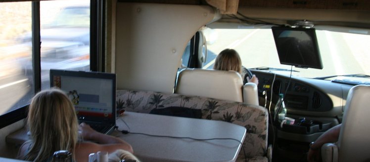
As for the latency – it is really small when using the appropriate video player. The in-camera latency is less than two frames (about 20 scanlines + 1000 pixels in the FPGA – from the sensor port to the compressed bitstream in the system memory buffer and one frame in the buffer before the frame is sent out). When using the MPlayer the host PC latency is also about just one frame that makes it possible to use the camera+PC in real time applications, like a replacement of a rear view mirror in Elphel mobile office
The article says that The imaging chip is taken from a Nokia N95 cell phone but it seems not to be complete. Yes, it may be (and likely is but I do not know for sure – N95 circuit diagram is not posted) the same imaging chip, but according to this posting the sensor front end board is really open source and you can download the documentation (released under GNU FDL license) from Elphel Wiki page
Update:Andrew, thank you for adding information to Frequently asked questions about the Frankencamera .
BTW – we were able to control Canon EOS lenses directly in our model 323C ("C" for "Canon"), we may still have some hardware around. And the code is at Sourceforge – lensraw.html , lensraw.c
September 3, 2009
by admin
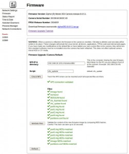
I just finished working on a new graphical user interface in the general camera system preferences that should simplify the process of camera firmware upgrade also called “reflashing”. There are quite a few ways to update a cameras firmware so it might be challenging to keep a clear overview: http://wiki.elphel.com/index.php?title=Usage_Tutorials.
The basic idea is the same for all approaches:
- Share a new firmware image on a computer over NFS (Tutorial on setting up NFS can be found here)
- Tell the camera the NFS share and start the reflash script
The new GUI should do this in a tidy manner and verifies that the share is working correctly and that all required firmware files are valid before letting you press the Reflash button.
August 28, 2009
by Oleg Dzhimiev
Notes:
- Commands can be ‘broadcasted’ through I2C to all the sensors.
- Sensors work only in snapshot (external trigger) mode – to have them configured identically.
- Depth frame mode.
- Direct alternating channels mode.
- Alternating channels – one channek direct, another – bufferred.
August 14, 2009
by Oleg Dzhimiev
There’s a nice page on Elphel’s wiki describes the problem: Adjusting sensor clock phase (the last paragraph is outdated, the script is in the ‘attic’, and I couldn’t find an alternative in the new 8.x firmware).
It was difficult to adjust data phases for long cables (& sometimes even for short) connecting sensor boards with 10359. To do it in a more or less automatic way a php script ‘test_inner_10359.php’ is used, which in its turn uses ‘phases_adjust.php’ with 5 phase steps at a time and compares the MD5 sums of the frames with the known one at defined sensor parameters.
So far, the solution is:
- The problem was with the sensor on J2 mostly. In 10359 project that sensor is clocked through the BUFG (idclk) by the clock coming from 10353 (DCLK) . After inverting it the things got better – and this is luck.
- In ‘phases_adjust.php” changed the number of phase steps taken from 5 to 2 to increase the precision. And it worked =) – 5/5 for the camera in the office.
TODO:
- Add an “AUTO” button to 10359 interface page.
- Modify standard (in prod353) ‘test_inner_10359.php’ to be able to work with only 2 sensors.
HOWTO:
- go to: http://<camera-ip>/359/10359_controls.html
PS: Also tried to add a bit mask to data bus from the sensor just to find out whether the data bus changing time exceeds the period but the picture became unstable every time the phase was close to the correct one.
July 15, 2009
by Oleg Dzhimiev
So far, the code works in the following way:
- Frames from sensor are stored in SDRAM, then the data go to the Cross-Correlation module.
- The output of the C-C module are 256 values for each pass cross-correlation function. The address (=pixel displacement) of the maximal value is written to a BRAM.
- After the whole picture line is processed the results are read out and form a line of a ‘depth frame’ that is sent to the main 353 board.
So, the ‘depth frame’ goes through the 353’s compressor and this makes the data available only for visual analysis. I’m planning:
- 353 will get optionally ‘depth frame’ OR frames from the left/right sensor.
- at the same time the ‘depth frame’ lines will be available through the I2C register – basically that means I’ll just duplicate the BRAM where I store the depth information.
Shall I keep the whole frame? shall I write it to the SDRAM? I’ll use 1 BRAM at first. Section 1 & 2 w/o ‘frames from the left/right sensor‘ will take less then an hour.
July 10, 2009
by Andrey Filippov
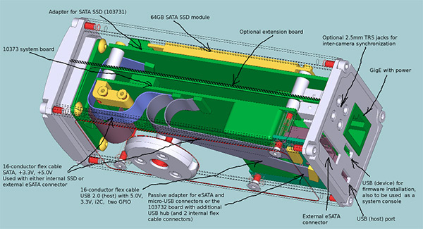
Spent couple days looking if the 10373 board layout can be connected as I hoped. There will be small board with 2 connectors on the back panel (103732) – micro USB and eSATA. In minimal configuration it will be a passive board with connectors only, but there should be some room to add USB hub and a couple internal 10-conductor flex cables for internal USB devices – same as on the 10369 board of the NC353L camera.
SATA and USB signals are split into separate connectors on the 10373 board – that allows to leave USB connected to the back panel adapter while connecting the SATA cable (with additional power) to the internal adapter for the SATA SSD. The image below shows both options, but actually 10373 has only one SATA port so only one SATA device can be connected.
While most functionality of the 10369 board is moved to the main 10373 there is no ports for the inter-camera synchronization – 10369 has 2 sets of oto-isolated synchronization ports – “external” with modular (like telephone) connector for frame-locking several individual cameras an “internal” (with flex cable connectors) for synchronizing multiple camera boards installed in the same enclosure. The synchronization will have to be handled by an extension board that has direct connection to the 18 FPGA I/O pins. The back panel will have holes (covered with plastic overlay when not used) for up to four 2.5mm TRS connectors (like small stereo audio ones). Unfortunately even small 2.5mm TRS plugs plastic bodies are rather large so 2 of them can fit only when connectors are diagonal.. Anyway – that part of the design is not finished yet, we’ll think of something.
Andrey
July 9, 2009
by Oleg Dzhimiev
1. [In Progress] “Verification of everything”.
The results of running 1 frame through the cross-correlation block are more or less ok now:
- took coefficients’ product bits [31:16] (that is 16 bit rounding)
Sample 1:

Fig.1 Source – test frame.

Fig. 2 Result (there are some errors on the top of the result image near the areas of color change).
Sample 2:
 Fig. 3 The picture from the sensor w/o a lense (a bit dirty – dust on scotch).

Fig. 4 Result, again there are some errors – overflows are possible.
TODO:
1. Adjust the more suitable rounding for fft-coeffs multiplication – perform rounding after multiplication + perform rounding in IFFT?
Current Bits Calculation: 12bits -> FFT(8 stages with rounding) -> 12bits -> MULT(16 bits rounding) -> 8bits -> IFFT(no rounding) -> 16bits.
Try: 12 -> FFT (8 cut) -> 12 -> MULT (8 cut)-> 16 -> IFFT(8 cut) -> 16 – and there should be no errors.
2. Test frames from different channels.
July 2, 2009
by Andrey Filippov
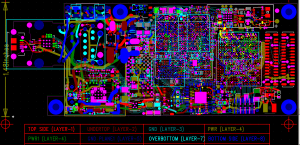
It seems that those additional parts did fit on the board. I still need to restore some power connections and the legend on the board (it is also getting to be a real challenge – the smallest letters have to use 0.125mm (5 mil) lines and there is very little space between the components. It will need some time, but it is definitely doable. This is how the board looks now (click on the image to get the full size):

So to the 10373 features I listed initially in my May, 18 post:
- TMS320DM6467 as the CPU
- Xilinx Spartan 6 FPGA
- 256 MiB NAND flash
- 256 MiB DDR2 system memory
- 256 MiB DDR3 dedicated FPGA memory
- 48V DC over Ethernet cable
- GigE
- USB 2.0 host
- ATA port (to be used with the SATA bridge on the 10369 or similar I/O board)
- USB 1.1 device with micro USB connector. It is connected to the CPU serial port to be used as a system console and alternative boot source
Few more can be added:
- Two sensor ports, each can accommodate existent sensor front ends that work with NC353L cameras. Both sensors will be able to operate at full resolution/speed in parallel.
- SATA port with the flex cable connector. The connector pinout is made so it is possible to use flexible cables (single-layer) , not just 2-layer cable or flex PCB to achieve 100 Ohm impedance for the high-speed differential pairs. On the other end of that cable there will be either eSATA connector on the back panel of the camera or an adapter for the 64GB SSD used in some EEE PC computers. As you can see on Elphel wiki these 64GB memory can easily fit inside the camera – so no more CF cards. Same with 1.8″ HDD – we can make an adapter from the same flex cable – it addition to SATA signals it has both 3.3VDC and 5VDC power.
- Another flex cable connector has USB 2.0 (host) signals, including 5V power and additional 3.3V and 4 GPIO signals from the FPGA. It is possible to put just micro USB connector adapter on the camera back panel (it is likely to be combined with the eSATA one to simplify mounting) or have a 4-port USB hub (similar to the one in the 10369 board) and additional flex-cable connectors for internal USB or I2C internal add-ons (i.e compass).
- Clock/calendar with a super-capacitor power backup, similar to the one in our current 10369A board, but with the additional function – 10373 makes use of the alarm of that clock (it can be set up to a week in the future). Alarm output is used to re-power the camera after it turned itself off (and it can now). DC-DC converters still consume several mA when turned off, but it will be possible to use the camera with a very small solar panel in the wilderness unattended – either periodically recording images to the internal memory or using USB cellular module (if the area has coverage) to upload the images.
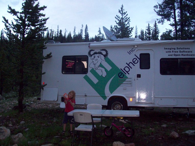
And here is where I’m working on this board – 110.965W 40.65168N. It is raining most of the time – day and night, so I have more time to work.

« Previous Page —
Next Page »
 Fig.1 A sample frame in the testbench is 2592×3 (to reduce verification time), “ivact” – vertical sync signal, “ihact” – horizontal sync signal, “pxdr” – pixel data. White numbers in ‘ivact’ line represent an appropriate channel.
 Fig.2 “framen” – frame enable register, allows work when ‘high’.


 Fig. 3 The picture from the sensor w/o a lense (a bit dirty – dust on scotch).
