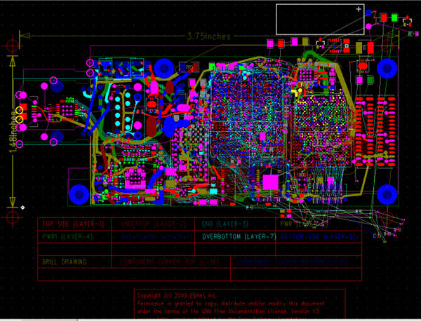
10373 – working on the PCB layout 2
After finishing the 10373 layout I did not feel satisfied – some valuable parts of the PCB were left wasted. When I was just starting this project I new I’ll have to use more layers (now 8, previous designs – 4), smaller traces (0.075 mm – down from 0.1mm) and use buried and blind vias that I never did before. And I still was not sure if everything will fit on the same board size, I even had a plan B for the system memory – use just one x16 chip and have lower bandwidth, but both chips did fit nicely (they are visible as large vertical rectangles just above the center of the board). And when I just started placement, I noticed that several hundred of huge 0402 resistors and capacitors will not actually fit around the chip with 0.4mm distnace between the pads. Each such resitor is longer than a millimiter, so I changed most of them (few do not exist in small package) to 0201 – that was better, just 0.6mm by 0.3mm. End everything did fit and some extra remained so I’m trying to put more of the useful components.
So I broke the layout, renamed the board to rev “A” (even as rev “0” was never build) and added few more connectors, ICs and other components and now I’m working on making the increased number of parts fit (some are still around the board, not yet placed). That huge supercapaitor on top (used for clock/calendar backup instead of a battery) will be placed over other components so it does not need that much empty space.
It will take me some time to fit everything, but it seems to be possible. And then the board will be really packed with no space wasted. And camera board – get more functionality even when no extension board will be installed.
Andrey

Could be the right time to add a video out feature 🙂
(only half kiding)
Philippe, “video out” is more a function of a monitor, not a camera. Only very old/low res. cameras had video signal inside anyway. And I do not feel enough resources to develop such a device and compete with so many existent devices that have screen, I would rather focus on the camera itself.
Of course, it is still possible to make a daughter board that will generate some kind of video output – now the connector for the extension board will be free again – most of the functionality of the 10369 board will be incorporated in the 10373itself , so that connector will be usually free and you will not have to give up SATA or USB to use it. And now there are more GPIOs from the FPGA there. You can also reuse the second sensor board connector, make it output instead of the input – internally all the signal pins go to the FPGA and their function is programmable.
But still the major part of the video output will be just the code (mostly FPGA one). It will be possible to use something like iphone (I don’t have one and don’t know it exact capabilities) to view the reduced resolution output even without any hardware modifications (that might be costly in low volume). It is very unlikely I’m going to do that personally, but I will be happy to answer any questions related to such a project.
Andrey